
Sign in
Sign up


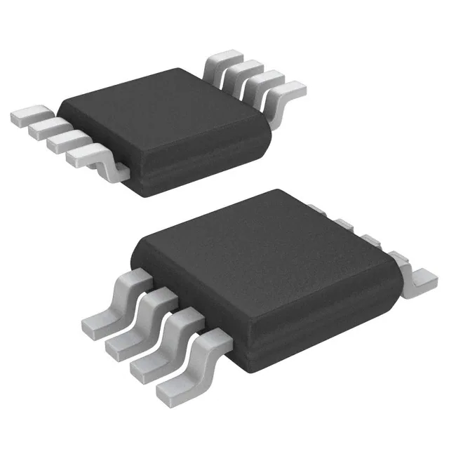
Images are for reference only , Please refer to the product datasheet
74CB3Q3306ADCURE4
3.3-V, 1:1 (SPST), 2-channel FET bus switch (active low)
Manufacturer:
Manufacturer NO:
74CB3Q3306ADCURE4
copy
Product SN:
10452-74CB3Q3306ADCURE4
copy
Package/Case:
-
copy
Manufacturer Lead Time:
-
copy
Datasheet:
Detailed Descripition:
Powered-off protection, Supports input voltage beyond supply
copy
Product Application Field:None
Product Application Field:None
Documents & Media
Datasheets PDF 74CB3Q3306ADCURE4 Datasheet PDF
Product Description
- High-Bandwidth Data Path (up to 500 MHz(1))
- 5-V-Tolerant I/Os With Device Powered Up or Powered Down
- Low and Flat ON-State Resistance (ron) Characteristics Over
Operating Range (ron = 4 Ω Typ) - Rail-to-Rail Switching on Data I/O Ports
- 0- to 5-V Switching With 3.3-V VCC
- 0- to 3.3-V Switching With 2.5-V VCC
- Bidirectional Data Flow With Near-Zero Propagation Delay
- Low Input/Output Capacitance Minimizes Loading and Signal Distortion
(Cio(OFF) = 3.5 pF Typ) - Fast Switching Frequency (f OE = 20 MHz Max)
- Data and Control Inputs Provide Undershoot Clamp Diodes
- Low Power Consumption (ICC = 0.25 mA Typ)
- VCC Operating Range From 2.3 V to 3.6 V
- Data I/Os Support 0- to 5-V Signaling Levels
(0.8 V, 1.2 V, 1.5 V, 1.8 V, 2.5 V, 3.3 V, 5 V) - Control Inputs Can Be Driven by TTL or 5-V/3.3-V CMOS Outputs
- Ioff Supports Partial-Power-Down Mode Operation
- Latch-Up Performance Exceeds 100 mA Per JESD 78, Class II
- ESD Performance Tested Per JESD 22
- 2000-V Human-Body Model (A114-B, Class II)
- 1000-V Charged-Device Model (C101)
- Supports Both Digital and Analog Applications: USB Interface, Differential Signal
Interface, Bus Isolation, Low-Distortion Signal Gating
0 In Stock
Finding Goods Through Sales
Want the lower wholesale price? Please send RFQ, we will respond immediately
Product price
No prices available at the moment
For more 74CB3Q3306ADCURE4 prices, contact customer service to get a discount!
You May Also Like


0 In Stock
Finding Goods Through Sales
Want the lower wholesale price? Please send RFQ, we will respond immediately
Product price
No prices available at the moment
For more 74CB3Q3306ADCURE4 prices, contact customer service to get a discount!
Home
Chat
Compare
Add To RFQ