
Sign in
Sign up


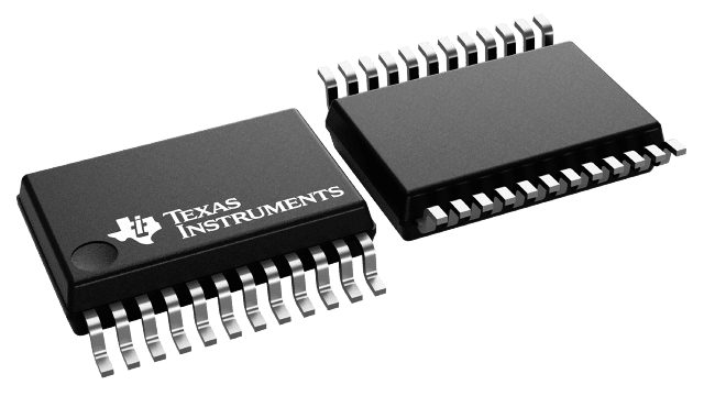
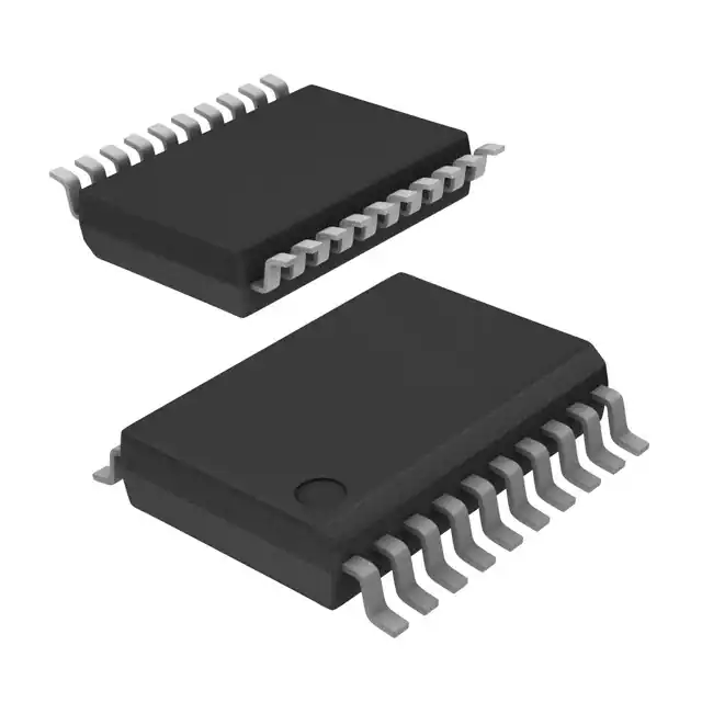
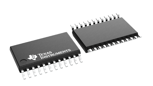
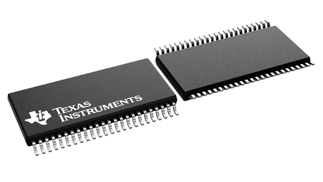
Images are for reference only , Please refer to the product datasheet
CDC351IDB
1-line to 10-line 3.3-V clock driver with tri-state outputs
Manufacturer:
Manufacturer NO:
CDC351IDB
copy
Product SN:
10426-CDC351IDB
copy
Package/Case:
SSOP (DB)-24
copy
Manufacturer Lead Time:
-
copy
Datasheet:
Detailed Descripition:
Pin control
copy
Product Application Field:None
Product Application Field:None
Documents & Media
Datasheets PDF CDC351IDB Datasheet PDF
Product Description
- Low Output Skew, Low Pulse Skew for Clock-Distribution and Clock-Generation Applications
- Operates at 3.3-V VCC
- LVTTL-Compatible Inputs and Outputs
- Supports Mixed-Mode Signal Operation (5-V Input and Output Voltages With 3.3-V VCC)
- Distributes One Clock Input to Ten Outputs
- Distributed VCC and Ground Pins Reduce Switching Noise
- High-Drive Outputs (-32-mA IOH, 32-mA IOL)
- State-of-the-Art EPIC-IIBTM BiCMOS Design Significantly Reduces Power Dissipation
- Package Options Include Plastic Small-Outline (DW) and Shrink Small-Outline (DB) Packages
0 In Stock
Finding Goods Through Sales
Want the lower wholesale price? Please send RFQ, we will respond immediately
Product price
Qty
Unit Price
Ext Price
1000
$6.688
$6688
For more CDC351IDB prices, contact customer service to get a discount!
You May Also Like


0 In Stock
Finding Goods Through Sales
Want the lower wholesale price? Please send RFQ, we will respond immediately
Product price
Qty
Unit Price
Ext Price
1000
$6.688
$6688
For more CDC351IDB prices, contact customer service to get a discount!
Home
Chat
Compare
Add To RFQ