
Sign in
Sign up


Images are for reference only , Please refer to the product datasheet
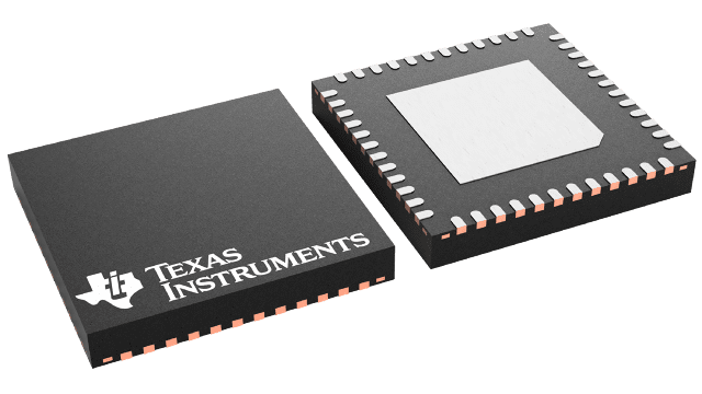
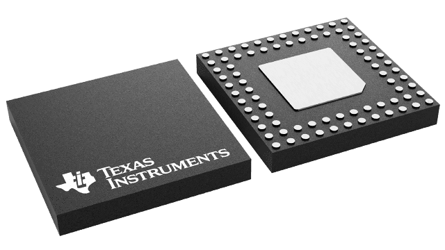
CDCLVD2108RGZT
48-VQFN (7x7) Low jitter, dual 1:8 universal-to-LVDS buffer
Manufacturer:
Manufacturer NO:
CDCLVD2108RGZT
copy
Product SN:
10426-CDCLVD2108RGZT
copy
Package/Case:
VQFN (RGZ)-48
copy
Manufacturer Lead Time:
6 Weeks
copy
Datasheet:
Detailed Descripition:
Dual 1:8 fanout, Output enable control, Universal inputs
copy
Product Application Field:None
Product Application Field:None
Environmental & Export Classifications
RoHS Status
ROHS3 Compliant
Moisture Sensitivity Level (MSL)
3 (168 Hours)
REACH Status
REACH Unaffected
ECCN
EAR99
HTSUS
8542.39.0001
Documents & Media
Datasheets PDF CDCLVD2108RGZT Datasheet PDF
Product Description
 transmission lines. In case of driving the inputs in single ended mode, the appropriate bias voltage (VAC_REF) should be applied to the unused negative input pin.
- Dual 1:8 Differential Buffer
- Low Additive Jitter <300 fs RMS in
10 kHz to 20 MHz - Low Within Bank Output Skew of 50 ps (Max)
- Universal Inputs Accept LVDS, LVPECL, LVCMOS
- One Input Dedicated for Eight Outputs
- Total of 16 LVDS Outputs, ANSI EIA/TIA-644A
Standard Compatible - Clock Frequency up to 800 MHz
- 2.375–2.625V Device Power Supply
- LVDS Reference Voltage, VAC_REF,
Available for Capacitive Coupled Inputs - Industrial Temperature Range –40°C to 85°C
- Packaged in 7mm × 7mm 48-Pin QFN (RGZ)
- ESD Protection Exceeds 3 kV HBM, 1 kV CDM
- APPLICATIONS
- Telecommunications/Networking
- Medical Imaging
- Test and Measurement Equipment
- Wireless Communications
- General Purpose Clocking
325 In Stock
Can Ship lmmediately
Want the lower wholesale price? Please send RFQ, we will respond immediately
Product price
Qty
Unit Price
Ext Price
1000
$6.653
$6653
For more CDCLVD2108RGZT prices, contact customer service to get a discount!
You May Also Like


325 In Stock
Can Ship lmmediately
Want the lower wholesale price? Please send RFQ, we will respond immediately
Product price
Qty
Unit Price
Ext Price
1000
$6.653
$6653
For more CDCLVD2108RGZT prices, contact customer service to get a discount!
Home
Chat
Compare
Add To RFQ