
Sign in
Sign up


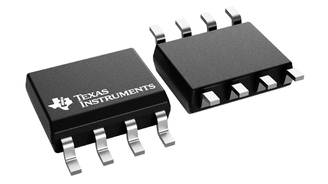
Images are for reference only , Please refer to the product datasheet
DAC7551TDRNRQ1
Automotive 12-Bit, Ultralow Glitch, Voltage Output Digital to Analog Converter
Manufacturer:
Manufacturer NO:
DAC7551TDRNRQ1
copy
Product SN:
10437-DAC7551TDRNRQ1
copy
Package/Case:
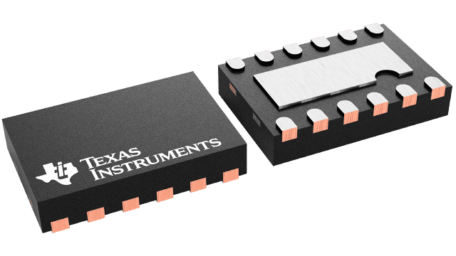
USON (DRN)-12
copy
Manufacturer Lead Time:
-
copy
Datasheet:
Detailed Descripition:
Low Power, SDO
copy
Product Application Field:None
Product Application Field:None
Documents & Media
Datasheets PDF DAC7551TDRNRQ1 Datasheet PDF
Product Description
- Qualified for Automotive Applications
- Relative Accuracy (INL): ±0.35 LSB
- Ultra-Low Glitch Energy: 0.1 nV-s
- Low-Power Operation: 100 µA at 2.7 V
- Power-On Reset-to-Zero Scale
- Power Supply: 2.7- to 5.5-V Single Supply
- Power-Down: 0.05 µA at 2.7 V
- 12-Bit Linearity and Monotonicity
- Rail-to-Rail Voltage Output
- Settling Time: 5 µs (Max)
- SPI-Compatible Serial Interface With Schmitt-
Trigger Input: Up to 50 MHz - Daisy-Chain Capability
- Asynchronous Hardware Clear-to-Zero Scale
- Specified Temperature Range:
–40°C to +105°C - Small, 2-mm × 3-mm, 12-Lead USON Package
- Z-Suffix Offers Improved Delamination
0 In Stock
Finding Goods Through Sales
Want the lower wholesale price? Please send RFQ, we will respond immediately
Product price
Qty
Unit Price
Ext Price
1000
$1.77
$1770
For more DAC7551TDRNRQ1 prices, contact customer service to get a discount!
You May Also Like

0 In Stock
Finding Goods Through Sales
Want the lower wholesale price? Please send RFQ, we will respond immediately
Product price
Qty
Unit Price
Ext Price
1000
$1.77
$1770
For more DAC7551TDRNRQ1 prices, contact customer service to get a discount!
Home
Chat
Compare
Add To RFQ