
Sign in
Sign up


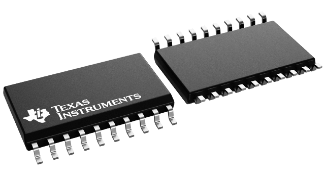
Images are for reference only , Please refer to the product datasheet
DAC8551AQDGKRQ1
DAC8551-Q1 Automotive 16-Bit, Ultralow-Glitch, Voltage-Output DAC
Manufacturer:
Manufacturer NO:
DAC8551AQDGKRQ1
copy
Product SN:
10437-DAC8551AQDGKRQ1
copy
Package/Case:
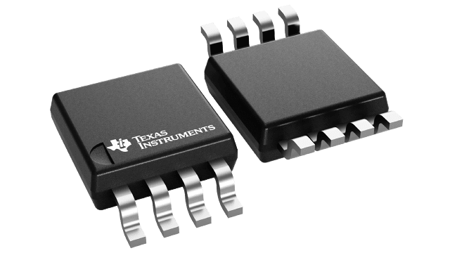
VSSOP (DGK)-8
copy
Manufacturer Lead Time:
-
copy
Datasheet:
Detailed Descripition:
Low Power
copy
Product Application Field:None
Product Application Field:None
Documents & Media
Datasheets PDF DAC8551AQDGKRQ1 Datasheet PDF
Product Description
- Qualified for Automotive Applications
- AEC-Q100 Qualified With the Following Results:
- Device Temperature Grade 1: –40°C to 125°C Ambient Operating Temperature Range
- Device HBM ESD Classification Level 2
- Device CDM ESD Classification Level C4B
- Relative Accuracy:
- DAC8551-Q1 (16-Bit): 4 LSB INL
- DAC6551-Q1 (12-Bit): 0.3 LSB INL
- Ultralow Glitch Impulse: 0.1 nV-s
- Settling Time: 8 µs to ±0.003% FSR
- Power Supply: 3 V to 5.5 V
- Power-On Reset to Zero Scale
- MicroPower Operation: 160 µA at 5 V
- Low-Power Serial Interface With Schmitt-Triggered Inputs
- On-Chip Output Buffer Amplifier With Rail-to-Rail Operation
- Power-Down Capability
- Binary Input
- SYNC Interrupt Facility
- Available in a Tiny VSSOP-8 Package
0 In Stock
Finding Goods Through Sales
Want the lower wholesale price? Please send RFQ, we will respond immediately
Product price
Qty
Unit Price
Ext Price
1000
$2.478
$2478
For more DAC8551AQDGKRQ1 prices, contact customer service to get a discount!
You May Also Like

0 In Stock
Finding Goods Through Sales
Want the lower wholesale price? Please send RFQ, we will respond immediately
Product price
Qty
Unit Price
Ext Price
1000
$2.478
$2478
For more DAC8551AQDGKRQ1 prices, contact customer service to get a discount!
Home
Chat
Compare
Add To RFQ