
Sign in
Sign up


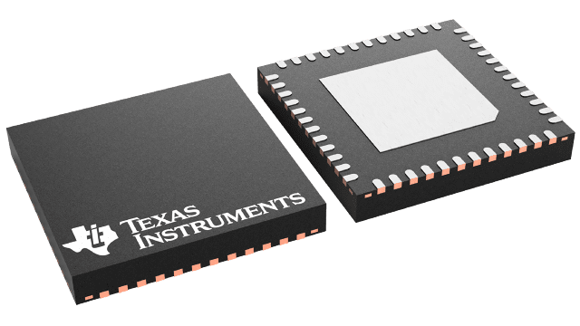
Images are for reference only , Please refer to the product datasheet
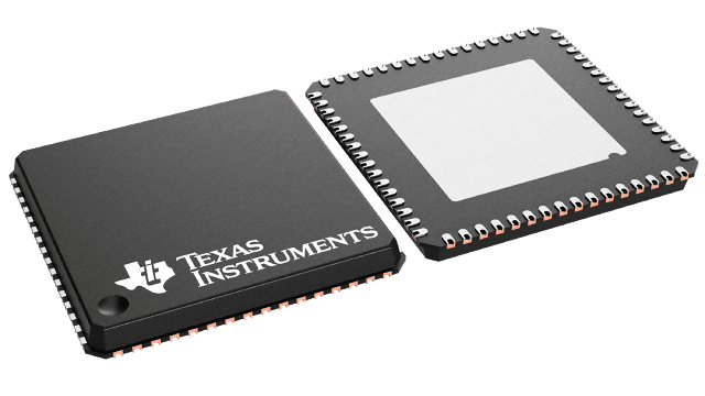
DS90C189TWRTDRQ1
64-VQFN (9x9) Low Power 1.8-V Dual Pixel FPD-Link (LVDS) Serializer
Manufacturer:
Manufacturer NO:
DS90C189TWRTDRQ1
copy
Product SN:
10464-DS90C189TWRTDRQ1
copy
Package/Case:
VQFNP (RTD)-64
copy
Manufacturer Lead Time:
12 Weeks
copy
Datasheet:
Detailed Descripition:
Low-EMI Point-to-Point Communication
copy
Product Application Field:None
Product Application Field:None
Environmental & Export Classifications
RoHS Status
ROHS3 Compliant
Moisture Sensitivity Level (MSL)
3 (168 Hours)
REACH Status
REACH Unaffected
ECCN
EAR99
HTSUS
8542.39.0001
Documents & Media
Datasheets PDF DS90C189TWRTDRQ1 Datasheet PDF
Product Description
- AEC-Q100 Qualified for Automotive Applications with the Following Specifications:
- Device Temperature Grade 2: –40°C to +105°C Ambient Operating Temperature
- Device HBM ESD Classification Level ±8 kV
- Device CDM ESD Classification Level ±750 V
- 150 mW Typical Power Consumption at 185 MHz (SIDO Mode)
- Drives QXGA and WQXGA Class Displays
- Two Operating Modes:
- Single Pixel In, Single Pixel Out (SISO): 105 MHz Maximum
- Single Pixel In, Dual Pixel Out (SIDO): 185 MHz Maximum
- Supports 24-Bit RGB
- Supports 3D+C, 4D+C, 6D+C, 6D+2C, 8D+C, and 8D+2C LVDS Configurations
- Compatible With FPD-Link Devices
- Operates Off a Single 1.8-V Supply
- Interfaces Directly With 1.8-V LVCMOS
- Less Than 10 mW Power Consumption in Sleep Mode
- Spread Spectrum Clock Compatible
- Small 9 mm × 9 mm × 0.9 mm 64-Pin VQFN Package
0 In Stock
Finding Goods Through Sales
Want the lower wholesale price? Please send RFQ, we will respond immediately
Product price
Qty
Unit Price
Ext Price
1000
$5.28
$5280
For more DS90C189TWRTDRQ1 prices, contact customer service to get a discount!
You May Also Like


0 In Stock
Finding Goods Through Sales
Want the lower wholesale price? Please send RFQ, we will respond immediately
Product price
Qty
Unit Price
Ext Price
1000
$5.28
$5280
For more DS90C189TWRTDRQ1 prices, contact customer service to get a discount!
Home
Chat
Compare
Add To RFQ