
Sign in
Sign up


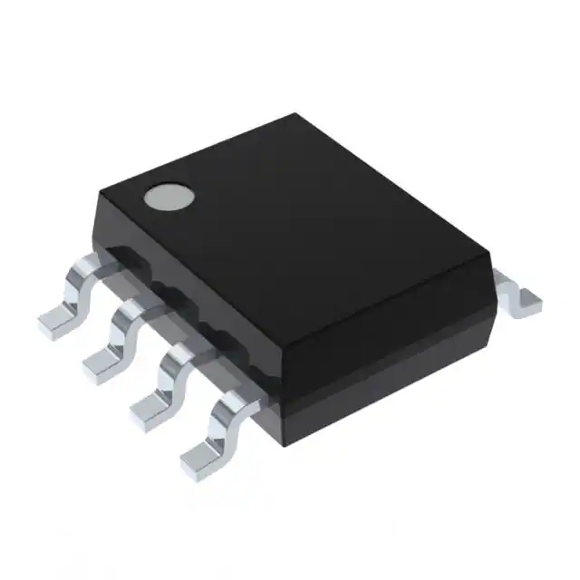
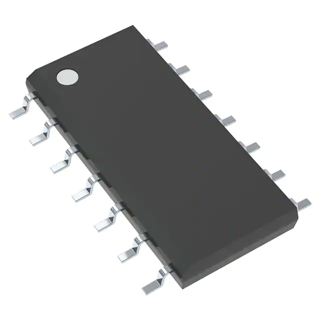
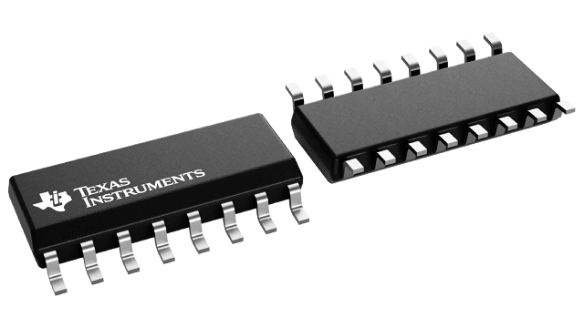
Images are for reference only , Please refer to the product datasheet
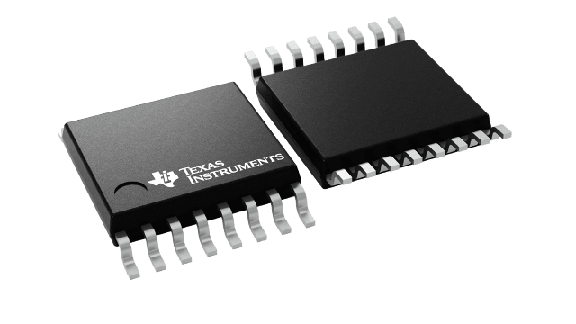
DSLVDS1047PWT
16-TSSOP 3.3-V LVDS quad channel high-speed differential line driver
Manufacturer:
Manufacturer NO:
DSLVDS1047PWT
copy
Product SN:
10456-DSLVDS1047PWT
copy
Package/Case:
TSSOP (PW)-16
copy
Manufacturer Lead Time:
6 Weeks
copy
Datasheet:
Detailed Descripition:
4/0 Driver LVDS 16-TSSOP
copy
Product Application Field:None
Product Application Field:None
Environmental & Export Classifications
RoHS Status
ROHS3 Compliant
Moisture Sensitivity Level (MSL)
1 (Unlimited)
REACH Status
REACH Unaffected
ECCN
EAR99
HTSUS
8542.39.0001
Documents & Media
Datasheets PDF DSLVDS1047PWT Datasheet PDF
Product Description
- Designed for Signaling Rates up to 400-Mbps
- 3.3-V Power Supply Design
- 300-ps Typical Differential Skew
- 400-ps Maximum Differential Skew
- 1.7-ns Maximum Propagation Delay
- ±350-mV Differential Signaling
- Low Power Dissipation (13 mW at 3.3-V Static)
- Interoperable With Existing 5-V LVDS Receivers
- High impedance on LVDS Outputs on Power Down
- Flow-Through Pinout Simplifies PCB Layout
- Meets or Exceeds TIA/EIA-644 LVDS Standard
- Industrial Operating Temperature Range
(−40°C to +85°C) - Available in TSSOP Package
89 In Stock
Can Ship lmmediately
Want the lower wholesale price? Please send RFQ, we will respond immediately
Product price
Qty
Unit Price
Ext Price
1000
$0.761
$761
For more DSLVDS1047PWT prices, contact customer service to get a discount!
You May Also Like


89 In Stock
Can Ship lmmediately
Want the lower wholesale price? Please send RFQ, we will respond immediately
Product price
Qty
Unit Price
Ext Price
1000
$0.761
$761
For more DSLVDS1047PWT prices, contact customer service to get a discount!
Home
Chat
Compare
Add To RFQ