
Sign in
Sign up


Images are for reference only , Please refer to the product datasheet
LMH6401IRMZT
4.5 GHz ultra wideband digital variable gain amplifier
Manufacturer:
Manufacturer NO:
LMH6401IRMZT
copy
Product SN:
10758-LMH6401IRMZT
copy
Package/Case:
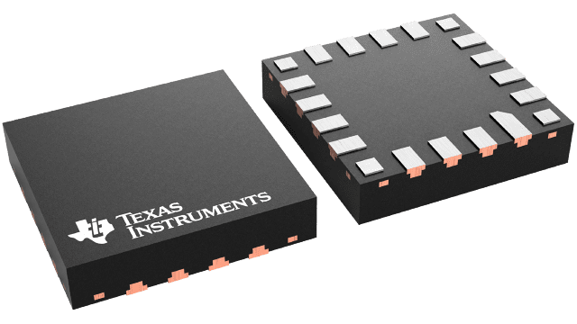
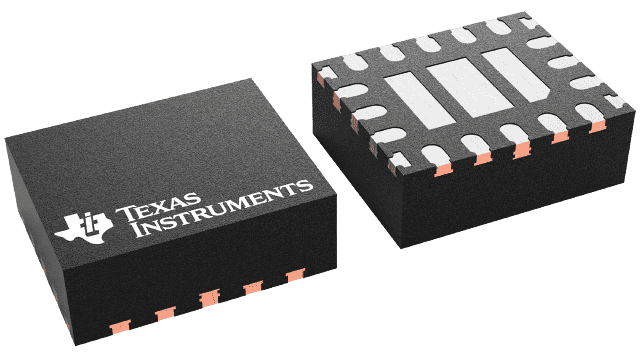
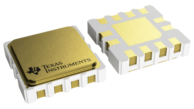
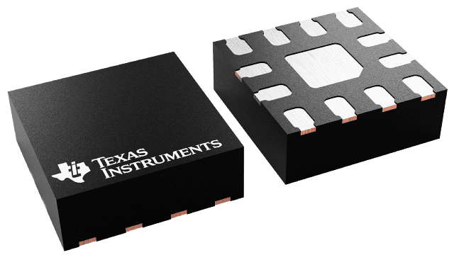
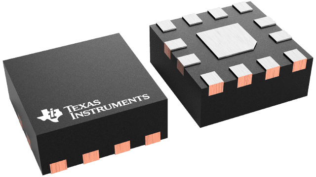
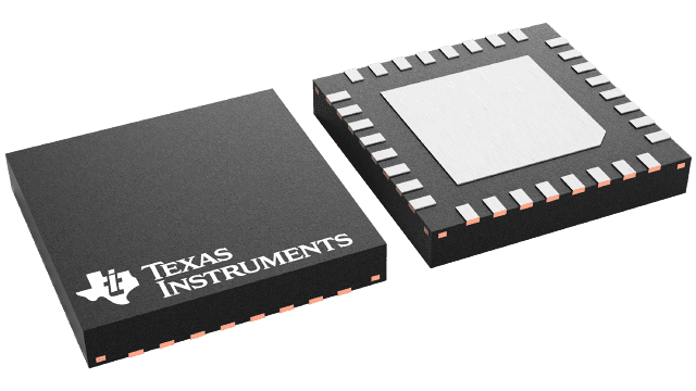
UQFN-HR (RMZ)-16
copy
Manufacturer Lead Time:
-
copy
Datasheet:
Detailed Descripition:
-
copy
Product Application Field:None
Product Application Field:None
Documents & Media
Datasheets PDF LMH6401IRMZT Datasheet PDF
Product Description
- 3-dB Bandwidth: 4.5 GHz at 26-dB Gain
- Gain Range: –6 dB to 26 dB in 1-dB Steps
- Differential Input Impedance: 100 Ω
- Differential Output with Common-Mode Control
- Distortion at Max Gain (VO = 2 VPPD, RL = 200 Ω):
- 200 MHz: HD2 at –73 dBc, HD3 at –80 dBc
- 500 MHz: HD2 at –68 dBc, HD3 at –72 dBc
- 1 GHz: HD2 at –63 dBc, HD3 at –63 dBc
- 2 GHz: HD2 at –58 dBc, HD3 at –54 dBc
- Output IP3:
- 43 dBm at 200 MHz
- 33 dBm at 1 GHz
- 27 dBm at 2 GHz
- Output IP2:
- 67 dBm at 200 MHz
- 60 dBm at 1 GHz
- 52 dBm at 2 GHz
- 8-dB Noise Figure at 1 GHz, RS = 100 Ω
- 82-ps Rise, Fall Time Pulse Response
- Supply Operation: 5.0 V at 69 mA
- Supports Single- and (±) Split-Supply Operation:
- DC- and AC-Coupled Applications
- Fabricated on an Advanced Complementary BiCMOS Process
- 3-mm × 3-mm UQFN-16 Package
0 In Stock
Finding Goods Through Sales
Want the lower wholesale price? Please send RFQ, we will respond immediately
Product price
Qty
Unit Price
Ext Price
1000
$11.558
$11558
For more LMH6401IRMZT prices, contact customer service to get a discount!
You May Also Like


0 In Stock
Finding Goods Through Sales
Want the lower wholesale price? Please send RFQ, we will respond immediately
Product price
Qty
Unit Price
Ext Price
1000
$11.558
$11558
For more LMH6401IRMZT prices, contact customer service to get a discount!
Home
Chat
Compare
Add To RFQ