
Sign in
Sign up


Images are for reference only , Please refer to the product datasheet
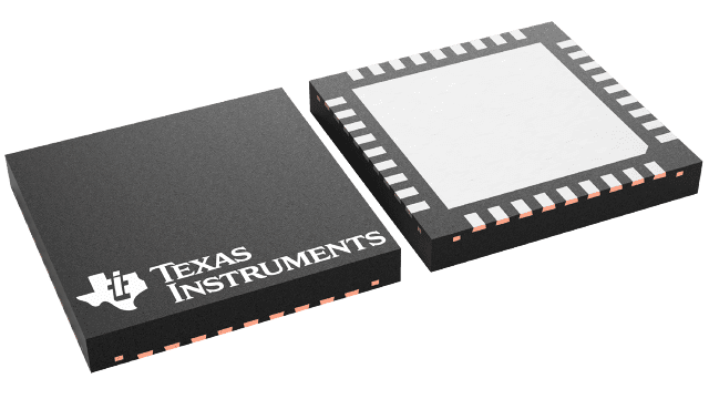
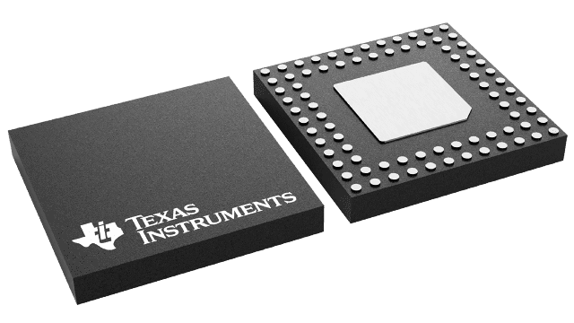
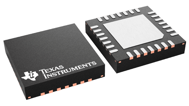
LMK00306SQX/NOPB
3.1-GHz differential clock buffer/level translator with 6 configurable outputs
Manufacturer:
Manufacturer NO:
LMK00306SQX/NOPB
copy
Product SN:
10426-LMK00306SQX/NOPB
copy
Package/Case:
WQFN (NJK)-36
copy
Manufacturer Lead Time:
-
copy
Datasheet:
Detailed Descripition:
Pin programmable
copy
Product Application Field:None
Product Application Field:None
Documents & Media
Datasheets PDF LMK00306SQX/NOPB Datasheet PDF
Product Description
- 3:1 Input Multiplexer
- Two Universal Inputs Operate up to 3.1 GHz
and Accept LVPECL, LVDS, CML, SSTL,
HSTL, HCSL, or Single-Ended Clocks - One Crystal Input Accepts a 10 to 40 MHz
Crystal or Single-Ended Clock
- Two Universal Inputs Operate up to 3.1 GHz
- Two Banks with 3 Differential Outputs Each
- LVPECL, LVDS, HCSL, or Hi-Z (Selectable
Per Bank) - LVPECL Additive Jitter with LMK03806 Clock
Source at 156.25 MHz:- 20 fs RMS (10 kHz to 1 MHz)
- 51 fs RMS (12 kHz to 20 MHz)
- LVPECL, LVDS, HCSL, or Hi-Z (Selectable
- High PSRR: –65 / –76 dBc (LVPECL/LVDS) at
156.25 MHz - LVCMOS Output with Synchronous Enable Input
- Pin-Controlled Configuration
- VCC Core Supply: 3.3 V ± 5%
- 3 Independent VCCO Output Supplies: 3.3 V/2.5 V
± 5% - Industrial Temperature Range: –40°C to +85°C
- 36-lead WQFN (6 mm × 6 mm)
0 In Stock
Finding Goods Through Sales
Want the lower wholesale price? Please send RFQ, we will respond immediately
Product price
Qty
Unit Price
Ext Price
1000
$3.313
$3313
For more LMK00306SQX/NOPB prices, contact customer service to get a discount!
You May Also Like


0 In Stock
Finding Goods Through Sales
Want the lower wholesale price? Please send RFQ, we will respond immediately
Product price
Qty
Unit Price
Ext Price
1000
$3.313
$3313
For more LMK00306SQX/NOPB prices, contact customer service to get a discount!
Home
Chat
Compare
Add To RFQ