
Sign in
Sign up


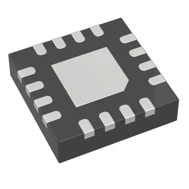
Images are for reference only , Please refer to the product datasheet
LMKDB1104Z85REXT
4-output LP-HCSL clock buffer for PCIe Gen 1 to Gen 6
Manufacturer:
Manufacturer NO:
LMKDB1104Z85REXT
copy
Product SN:
10426-LMKDB1104Z85REXT
copy
Package/Case:
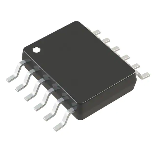
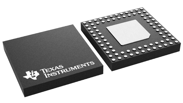
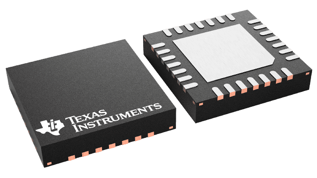
VQFN (REX)-28
copy
Manufacturer Lead Time:
-
copy
Datasheet:
Detailed Descripition:
1:20 fanout, Individual output enable control, OE# control, SMBus control, Side-Band Interface
copy
Product Application Field:None
Product Application Field:None
Documents & Media
Datasheets PDF LMKDB1104Z85REXT Datasheet PDF
Product Description
- LP-HCSL clock buffer and clock MUX that support:
- PCIe Gen 1 to Gen 6
- CC (Common Clock) and IR (Independent Reference) PCIe architectures
- Input clock with or without SSC
- DB2000QL compliant:
- All devices meet DB2000QL specifications
- LMKDB1120 is pin-compatible to DB2000QL
- Extremely low additive jitter:
- 31fs maximum 12kHz to 20MHz RMS additive jitter at 156.25MHz
- 13fs maximum additive jitter for PCIe Gen 4
- 5fs maximum additive jitter for PCIe Gen 5
- 3fs maximum additive jitter for PCIe Gen 6
- Fail-safe input
- Flexible power-up sequence
- Automatic output disable
- Individual output enable
- SBI (Side Band Interface) for high-speed output enable or disable
- LOS (Loss of Signal) input detection
- 85Ω or 100Ω output impedance
- 1.8V / 3.3V ± 10% power supply
- –40°C to 105°C ambient temperature
0 In Stock
Finding Goods Through Sales
Want the lower wholesale price? Please send RFQ, we will respond immediately
Product price
Qty
Unit Price
Ext Price
1000
$1.488
$1488
For more LMKDB1104Z85REXT prices, contact customer service to get a discount!
You May Also Like


0 In Stock
Finding Goods Through Sales
Want the lower wholesale price? Please send RFQ, we will respond immediately
Product price
Qty
Unit Price
Ext Price
1000
$1.488
$1488
For more LMKDB1104Z85REXT prices, contact customer service to get a discount!
Home
Chat
Compare
Add To RFQ