
Sign in
Sign up


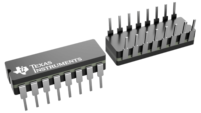
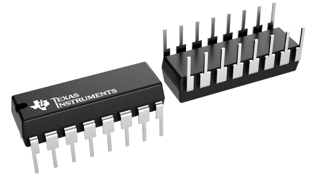
Images are for reference only , Please refer to the product datasheet
M38510/05152BEA
CMOS Dual J-K Master-Slave Flip-Flop
Manufacturer:
Manufacturer NO:
M38510/05152BEA
copy
Product SN:
10481-M38510/05152BEA
copy
Package/Case:
CDIP (J)-16
copy
Manufacturer Lead Time:
-
copy
Datasheet:
Detailed Descripition:
Balanced outputs, Clear, Positive edge triggered, Positive input clamp diode, Preset, Standard speed (tpd > 50ns)
copy
Product Application Field:None
Product Application Field:None
Documents & Media
Datasheets PDF M38510/05152BEA Datasheet PDF
Product Description
- Set-reset capability
- Static flip-flop operation – retains state indefinitely with clock level either high or low
- Medium speed operation – 16 MHz (typical) clock toggle rate at 10 V
- Standardized symmetrical output characteristics
- 100% tested for quiescent current at 20 V
- Maximum input current of 1 µA at 18 V over full package-temperature range; 100 nA at 18 V and 25°C
- Noise margin (over full package-temperature range):
- 1 V at VDD = 5 V
- 2 V at VDD = 10 V
- 2.5 V at VDD = 15 V
- 5 V, 10 V, and 15 V parametric ratings
- Meets all requirements of JEDEC tentative standard No. 138, standard specifications for description of ’B’ series CMOS devices
0 In Stock
Finding Goods Through Sales
Want the lower wholesale price? Please send RFQ, we will respond immediately
Product price
Qty
Unit Price
Ext Price
1000
$44.1
$44100
For more M38510/05152BEA prices, contact customer service to get a discount!
You May Also Like

0 In Stock
Finding Goods Through Sales
Want the lower wholesale price? Please send RFQ, we will respond immediately
Product price
Qty
Unit Price
Ext Price
1000
$44.1
$44100
For more M38510/05152BEA prices, contact customer service to get a discount!
Home
Chat
Compare
Add To RFQ