
Sign in
Sign up


Images are for reference only , Please refer to the product datasheet
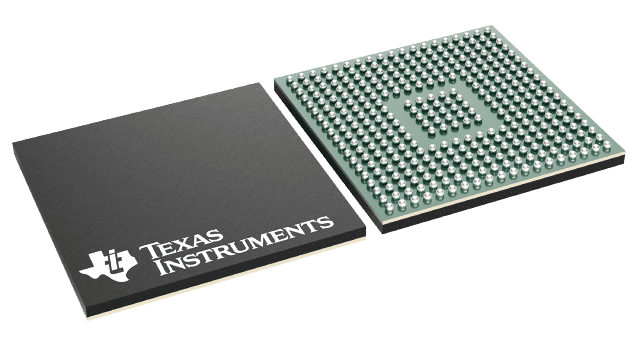
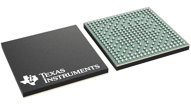
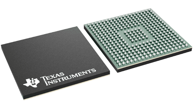
RM48L952DZWTT
16/32-Bit RISC Flash Microcontroller
Manufacturer:
Manufacturer NO:
RM48L952DZWTT
copy
Product SN:
10445-RM48L952DZWTT
copy
Package/Case:
NFBGA (ZWT)-337
copy
Manufacturer Lead Time:
-
copy
Datasheet:
Detailed Descripition:
Hercules high-performance microcontroller
copy
Product Application Field:None
Product Application Field:None
Documents & Media
Datasheets PDF RM48L952DZWTT Datasheet PDF
Product Description
- High-Performance Microcontroller for Safety-Critical Applications
- Dual CPUs Running in Lockstep
- ECC on Flash and RAM Interfaces
- Built-In Self-Test (BIST) for CPU and On-chip RAMs
- Error Signaling Module With Error Pin
- Voltage and Clock Monitoring
- ARM Cortex-R4F 32-Bit RISC CPU
- Efficient 1.66 DMIPS/MHz With 8-Stage Pipeline
- FPU With Single- and Double-Precision
- 12-Region Memory Protection Unit (MPU)
- Open Architecture With Third-Party Support
- Operating Conditions
- System Clock up to 220 MHz
- Core Supply Voltage (VCC): 1.2 V Nominal
- I/O Supply Voltage (VCCIO): 3.3 V Nominal
- ADC Supply Voltage (VCCAD): 3.0 to 5.25 V
- Integrated Memory
- 3MB of Program Flash With ECC
- 256KB of RAM With ECC
- 64KB of Flash With ECC for Emulated EEPROM
- 16-Bit External Memory Interface
- Common Platform Architecture
- Consistent Memory Map Across Family
- Real-Time Interrupt (RTI) Timer OS Timer
- 96-Channel Vectored Interrupt Module (VIM)
- 2-Channel Cyclic Redundancy Checker (CRC)
- Direct Memory Access (DMA) Controller
- 16 Channels and 32 Peripheral Requests
- Parity Protection for Control Packet RAM
- DMA Accesses Protected by Dedicated MPU
- Frequency-Modulated Phase-Locked Loop (FMPLL) With Built-In Slip Detector
- Separate Nonmodulating PLL
- Trace and Calibration Capabilities
- Embedded Trace Macrocell (ETM-R4)
- Data Modification Module (DMM)
- RAM Trace Port (RTP)
- Parameter Overlay Module (POM)
- Multiple Communication Interfaces
- 10/100 Mbps Ethernet MAC (EMAC)
- IEEE 802.3 Compliant (3.3-V I/O Only)
- Supports MII, RMII, and MDIO
- USB
- 2-Port USB Host Controller
- One Full-Speed USB Device Port
- Three CAN Controllers (DCANs)
- 64 Mailboxes, Each With Parity Protection
- Compliant to CAN Protocol Version 2.0B
- Standard Serial Communication Interface (SCI)
- Local Interconnect Network (LIN) Interface Controller
- Compliant to LIN Protocol Version 2.1
- Can be Configured as a Second SCI
- Inter-Integrated Circuit (I2C)
- Three Multibuffered Serial Peripheral Interfaces (MibSPIs)
- 128 Words With Parity Protection Each
- Two Standard Serial Peripheral Interfaces (SPIs)
- 10/100 Mbps Ethernet MAC (EMAC)
- Two Next Generation High-End Timer (N2HET) Modules
- N2HET1: 32 Programmable Channels
- N2HET2: 18 Programmable Channels
- 160-Word Instruction RAM Each With Parity Protection
- Each N2HET Includes Hardware Angle Generator
- Dedicated High-End Transfer Unit (HTU) With MPU for Each N2HET
- Two 12-Bit Multibuffered ADC Modules
- ADC1: 24 Channels
- ADC2: 16 Channels Shared With ADC1
- 64 Result Buffers With Parity Protection Each
- General-Purpose Input/Output (GPIO) Pins Capable of Generating Interrupts
- 16 Pins on the ZWT Package
- 10 Pins on the PGE Package
- IEEE 1149.1 JTAG, Boundary Scan and ARM CoreSight Components
- JTAG Security Module
- Packages
- 144-Pin Quad Flatpack (PGE) [Green]
- 337-Ball Grid Array (ZWT) [Green]
0 In Stock
Finding Goods Through Sales
Want the lower wholesale price? Please send RFQ, we will respond immediately
Product price
Qty
Unit Price
Ext Price
1000
$23.927
$23927
For more RM48L952DZWTT prices, contact customer service to get a discount!
You May Also Like


0 In Stock
Finding Goods Through Sales
Want the lower wholesale price? Please send RFQ, we will respond immediately
Product price
Qty
Unit Price
Ext Price
1000
$23.927
$23927
For more RM48L952DZWTT prices, contact customer service to get a discount!
Home
Chat
Compare
Add To RFQ