
Sign in
Sign up


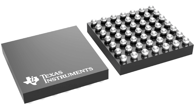
Images are for reference only , Please refer to the product datasheet
SN65LVDS311YFFT
49-DSBGA (2.8x2.8) Programmable 27-bit display serial interface transmitter
Manufacturer:
Manufacturer NO:
SN65LVDS311YFFT
copy
Product SN:
10467-SN65LVDS311YFFT
copy
Package/Case:
DSBGA (YFF)-49
copy
Manufacturer Lead Time:
6 Weeks
copy
Datasheet:
Detailed Descripition:
Cell Phone Interface 49-DSBGA (2.8x2.8)
copy
Product Application Field:None
Product Application Field:None
Environmental & Export Classifications
RoHS Status
ROHS3 Compliant
Moisture Sensitivity Level (MSL)
1 (Unlimited)
REACH Status
REACH Unaffected
ECCN
EAR99
HTSUS
8542.39.0001
Documents & Media
Datasheets PDF SN65LVDS311YFFT Datasheet PDF
Product Description
- 2.8 × 2.8mm package size
- 1.8V input signal swing
- 24-Bit RGB Data, 3 Control Bits, 1 Parity Bit and 2 Reserved Bits
Transmitted over 1, 2 or 3 Differential Lines - SubLVDS Differential Voltage Levels
- Three Operating Modes to Conserve Power
- Active-Mode QVGA 17.4mW (typ)
- Active-Mode VGA 28.8mW (typ)
- Shutdown Mode ≈ 0.5µA (typ)
- Standby Mode ≈ 0.5µA (typ)
- ESD Rating > 3kV (HBM)
- Pixel Clock Range of 4MHz–65MHz
- Failsafe on all CMOS Inputs
- Typical Application: Cameras, Embedded Computers
163 In Stock
Can Ship lmmediately
Want the lower wholesale price? Please send RFQ, we will respond immediately
Product price
Qty
Unit Price
Ext Price
1000
$2.218
$2218
For more SN65LVDS311YFFT prices, contact customer service to get a discount!
You May Also Like


163 In Stock
Can Ship lmmediately
Want the lower wholesale price? Please send RFQ, we will respond immediately
Product price
Qty
Unit Price
Ext Price
1000
$2.218
$2218
For more SN65LVDS311YFFT prices, contact customer service to get a discount!
Home
Chat
Compare
Add To RFQ