
Sign in
Sign up


Images are for reference only , Please refer to the product datasheet
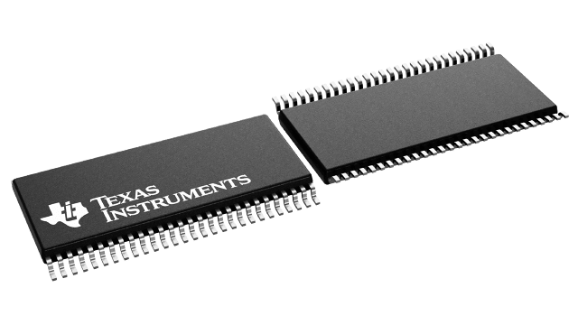
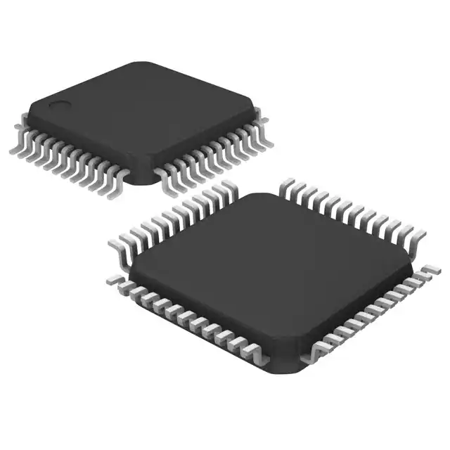
SN65LVDS93AIDGGRQ1
56-TSSOP 10MHz – 135MHz 28-bit Flat Panel Display Link LVDS SerDes Transmitter
Manufacturer:
Manufacturer NO:
SN65LVDS93AIDGGRQ1
copy
Product SN:
10464-SN65LVDS93AIDGGRQ1
copy
Package/Case:
TSSOP (DGG)-56
copy
Manufacturer Lead Time:
6 Weeks
copy
Datasheet:
Detailed Descripition:
Capable to Drive up to 10 meters STP Cable
copy
Product Application Field:None
Product Application Field:None
Environmental & Export Classifications
RoHS Status
ROHS3 Compliant
Moisture Sensitivity Level (MSL)
2 (1 Year)
REACH Status
REACH Unaffected
ECCN
EAR99
HTSUS
8542.39.0001
Documents & Media
Datasheets PDF SN65LVDS93AIDGGRQ1 Datasheet PDF
Product Description
- AEC-Q100 Qualified with:
- Temperature Grade 3: –40°C to 85°C
- HBM ESD Classification 3
- CDM ESD Classification C6
- LVDS Display Series Interfaces Directly to LCD
Display Panels With Integrated LVDS - Package: 14-mm × 6.1-mm TSSOP
- 1.8-V Up to 3.3-V Tolerant Data Inputs to Connect
Directly to Low-Power, Low-Voltage Application
and Graphic Processors - Transfer Rate up to 135 Mpps (Mega Pixel Per
Second); Pixel Clock Frequency Range 10 MHz to
135 MHz - Suited for Display Resolutions Ranging From
HVGA up to HD With Low EMI - Operates From a Single 3.3-V Supply and 170
mW (Typical) at 75 MHz - 28 Data Channels Plus Clock in Low-Voltage TTL
to 4 Data Channels Plus Clock Out Low-Voltage
Differential - Consumes Less Than 1 mW When Disabled
- Selectable Rising or Falling Clock Edge Triggered
Inputs - Support Spread Spectrum Clocking (SSC)
- Compatible with all OMAP™ 2x, OMAP™ 3x, and
DaVinci™ Application Processors
1740 In Stock
Can Ship lmmediately
Want the lower wholesale price? Please send RFQ, we will respond immediately
Product price
Qty
Unit Price
Ext Price
1000
$4.366
$4366
For more SN65LVDS93AIDGGRQ1 prices, contact customer service to get a discount!
You May Also Like


1740 In Stock
Can Ship lmmediately
Want the lower wholesale price? Please send RFQ, we will respond immediately
Product price
Qty
Unit Price
Ext Price
1000
$4.366
$4366
For more SN65LVDS93AIDGGRQ1 prices, contact customer service to get a discount!
Home
Chat
Compare
Add To RFQ