
Sign in
Sign up


Images are for reference only , Please refer to the product datasheet
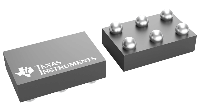
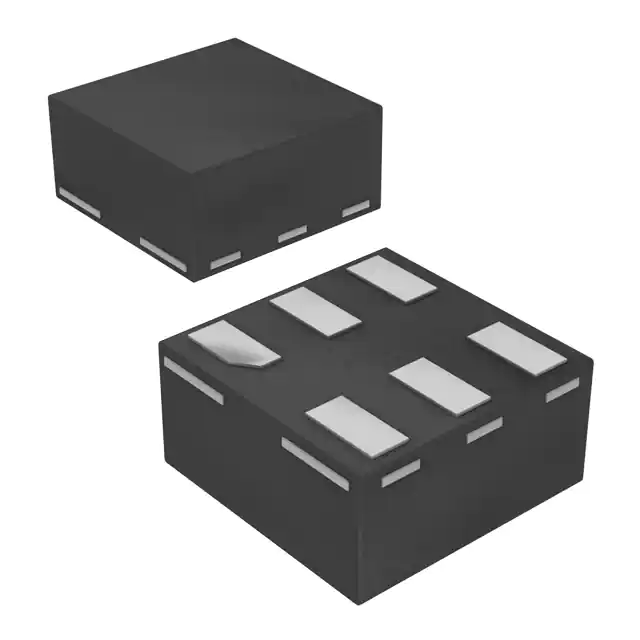
SN74AUP1T97YZPR
6-DSBGA Single-Supply Voltage Translator
Manufacturer:
Manufacturer NO:
SN74AUP1T97YZPR
copy
Product SN:
10490-SN74AUP1T97YZPR
copy
Package/Case:
DSBGA (YZP)-6
copy
Manufacturer Lead Time:
6 Weeks
copy
Datasheet:
Detailed Descripition:
Over-voltage tolerant inputs, Partial power down (Ioff), Single supply, Voltage translation
copy
Product Application Field:None
Product Application Field:None
Environmental & Export Classifications
RoHS Status
ROHS3 Compliant
Moisture Sensitivity Level (MSL)
1 (Unlimited)
REACH Status
REACH Unaffected
ECCN
EAR99
HTSUS
8542.39.0001
Documents & Media
Datasheets PDF SN74AUP1T97YZPR Datasheet PDF
Product Description
- Available in the Texas Instruments NanoStar™ Packages
- Single-Supply Voltage Translator
- 1.8 V to 3.3 V (at VCC = 3.3 V)
- 2.5 V to 3.3 V (at VCC = 3.3 V)
- 1.8 V to 2.5 V (at VCC = 2.5 V)
- 3.3 V to 2.5 V (at VCC = 2.5 V)
- Nine Configurable Gate Logic Functions
- Schmitt-Trigger Inputs Reject Input Noise and Provide Better Output Signal Integrity
- Ioff Supports Partial-Power-Down Mode With Low Leakage Current (0.5 µA)
- Very Low Static and Dynamic Power Consumption
- Pb-Free Packages Available: SON (DRY or DSF), SOT-23 (DBV), SC-70 (DCK), and NanoStar WCSP
- Latch-Up Performance Exceeds 100 mA Per JESD 78, Class II
- ESD Performance Tested Per JESD 22
- 2000-V Human-Body Model (A114-B, Class II)
- 1000-V Charged-Device Model (C101)
- Related Devices: SN74AUP1T98, SN74AUP1T57, and SN74AUP1T58
9 In Stock
Can Ship lmmediately
Want the lower wholesale price? Please send RFQ, we will respond immediately
Product price
Qty
Unit Price
Ext Price
1000
$0.095
$95
For more SN74AUP1T97YZPR prices, contact customer service to get a discount!
You May Also Like


9 In Stock
Can Ship lmmediately
Want the lower wholesale price? Please send RFQ, we will respond immediately
Product price
Qty
Unit Price
Ext Price
1000
$0.095
$95
For more SN74AUP1T97YZPR prices, contact customer service to get a discount!
Home
Chat
Compare
Add To RFQ