
Sign in
Sign up


Images are for reference only , Please refer to the product datasheet
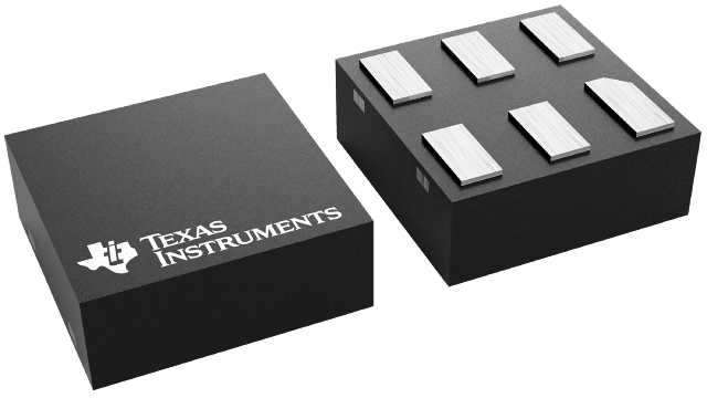
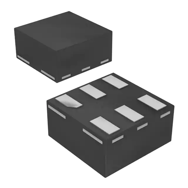
SN74AXC1T45DEAR
6-X2SON (1x1) Single-bit dual-supply bus transceiver
Manufacturer:
Manufacturer NO:
SN74AXC1T45DEAR
copy
Product SN:
10490-SN74AXC1T45DEAR
copy
Package/Case:
X2SON (DEA)-6
copy
Manufacturer Lead Time:
6 Weeks
copy
Datasheet:
Detailed Descripition:
Output enable, Overvoltage tolerant inputs, Partial power down (Ioff), Vcc isolation
copy
Product Application Field:None
Product Application Field:None
Environmental & Export Classifications
RoHS Status
ROHS3 Compliant
Moisture Sensitivity Level (MSL)
1 (Unlimited)
REACH Status
REACH Unaffected
ECCN
EAR99
HTSUS
8542.39.0001
Documents & Media
Datasheets PDF SN74AXC1T45DEAR Datasheet PDF
Product Description
- Up and down translation across 0.65 V to 3.6 V
- Operating temperature: –40°C to +125°C
- Designed with glitch suppression circuitry to improve power sequencing performance
- Maximum quiescent current (ICCA + ICCB) of 10µA (85°C maximum) and 16µA (125°C maximum)
- Up to 500Mbps support when translating from 1.8 to 3.3V
- VCC isolation feature:
- If either VCC input is below 100mV, all I/Os outputs are disabled and become high-impedance
- Ioff supports partial-power-down mode operation
- Latch-up performance exceeds 100mA per JESD 78, Class II
- ESD protection exceeds JESD 22:
- 8000-V human body model
- 1000-V charged-device model
20966 In Stock
Can Ship lmmediately
Want the lower wholesale price? Please send RFQ, we will respond immediately
Product price
Qty
Unit Price
Ext Price
1000
$0.099
$99
For more SN74AXC1T45DEAR prices, contact customer service to get a discount!
You May Also Like


20966 In Stock
Can Ship lmmediately
Want the lower wholesale price? Please send RFQ, we will respond immediately
Product price
Qty
Unit Price
Ext Price
1000
$0.099
$99
For more SN74AXC1T45DEAR prices, contact customer service to get a discount!
Home
Chat
Compare
Add To RFQ