
Sign in
Sign up


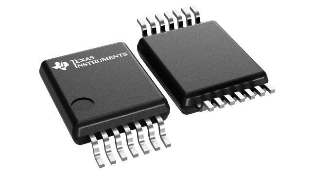
Images are for reference only , Please refer to the product datasheet
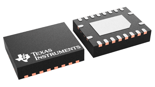
SN74CB3Q3245RGYR
3.3-V, 1:1 (SPST), 8-channel FET bus switch
Manufacturer:
Manufacturer NO:
SN74CB3Q3245RGYR
copy
Product SN:
10452-SN74CB3Q3245RGYR
copy
Package/Case:
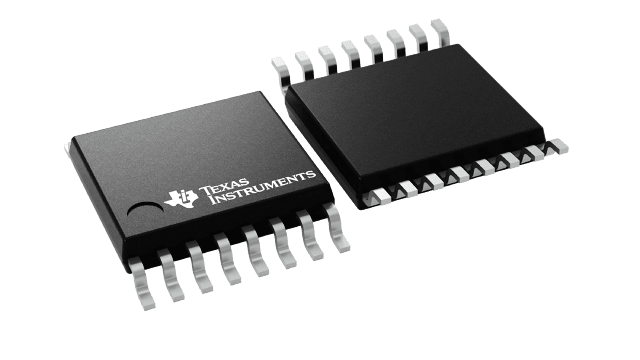
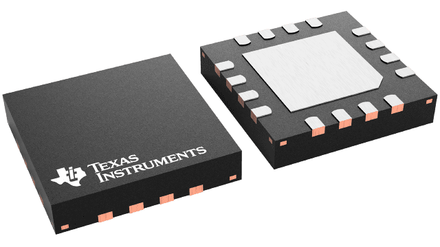
VQFN (RGY)-20
copy
Manufacturer Lead Time:
-
copy
Datasheet:
Detailed Descripition:
Powered-off protection, Supports input voltage beyond supply
copy
Product Application Field:None
Product Application Field:None
Documents & Media
Datasheets PDF SN74CB3Q3245RGYR Datasheet PDF
Product Description
- High-Bandwidth Data Path (Up to 500 MHz
 )
) - Equivalent to IDTQS3VH384 Device
- 5-V Tolerant I/Os with Device Powered-Up or Powered-Down
- Low and Flat ON-State Resistance (ron) Characteristics Over Operating Range (ron = 4
 Typical)
 - Rail-to-Rail Switching on Data I/O Ports
- 0- to 5-V Switching With 3.3-V VCC
- 0- to 3.3-V Switching With 2.5-V VCC
- Bidirectional Data Flow, With Near-Zero Propagation Delay
- Low Input/Output Capacitance Minimizes Loading and Signal Distortion (Cio(OFF) = 3.5 pF Typical)
- Fast Switching Frequency (fOE\ = 20 MHz Max)
- Data and Control Inputs Provide Undershoot Clamp Diodes
- Low Power Consumption (ICC = 1 mA Typical)
- VCC Operating Range From 2.3 V to 3.6 V
- Data I/Os Support 0 to 5-V Signaling Levels (0.8-V, 1.2-V, 1.5-V, 1.8-V, 2.5-V, 3.3-V, 5-V)
- Control Inputs Can be Driven by TTL or 5-V/3.3-V CMOS Outputs
- Ioff Supports Partial-Power-Down Mode Operation
- Latch-Up Performance Exceeds 100 mA Per JESD 78, Class II
- ESD Performance Tested Per JESD 22
- 2000-V Human-Body Model (A114-B, Class II)
- 1000-V Charged-Device Model (C101)
- Supports Both Digital and Analog Applications: PCI Interface, Differential Signal Interface, Memory Interleaving, Bus Isolation, Low-Distortion Signal Gating
0 In Stock
Finding Goods Through Sales
Want the lower wholesale price? Please send RFQ, we will respond immediately
Product price
Qty
Unit Price
Ext Price
1000
$0.319
$319
For more SN74CB3Q3245RGYR prices, contact customer service to get a discount!
You May Also Like


0 In Stock
Finding Goods Through Sales
Want the lower wholesale price? Please send RFQ, we will respond immediately
Product price
Qty
Unit Price
Ext Price
1000
$0.319
$319
For more SN74CB3Q3245RGYR prices, contact customer service to get a discount!
Home
Chat
Compare
Add To RFQ