
Sign in
Sign up


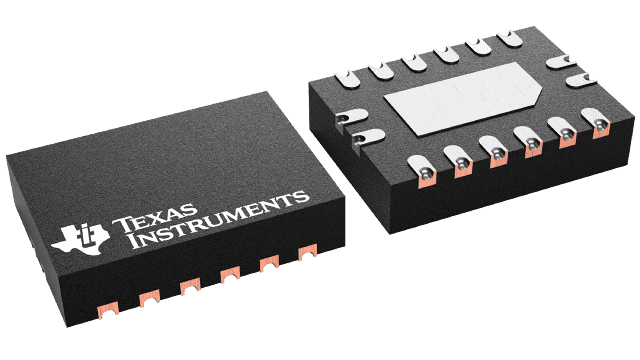
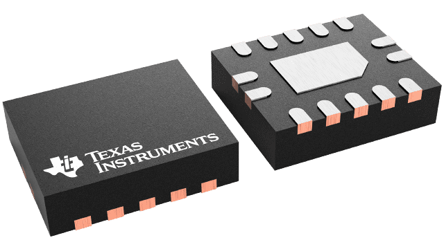
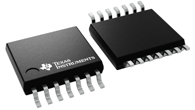
Images are for reference only , Please refer to the product datasheet
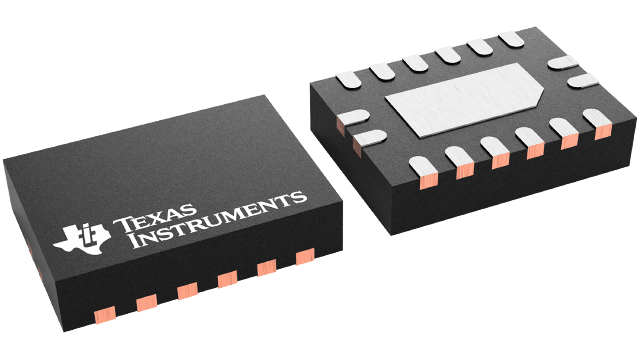
SN74LV8T596BQBR
Eight-bit voltage translating shift registers
Manufacturer:
Manufacturer NO:
SN74LV8T596BQBR
copy
Product SN:
10487-SN74LV8T596BQBR
copy
Package/Case:
WQFN (BQB)-16
copy
Manufacturer Lead Time:
-
copy
Datasheet:
Detailed Descripition:
-
copy
Product Application Field:None
Product Application Field:None
Documents & Media
Datasheets PDF SN74LV8T596BQBR Datasheet PDF
Product Description
- Latching logic with known power-up state provides consistent start-up behavior
- Wide operating range of 1.65V to 5.5V
- 5.5V tolerant input pins
- LVxT enhanced inputs combined with open-drain outputs provide maximum voltage translation flexibility:
- Over 6.67Mbps operation, (RPU = 1kΩ,CL = 30pF)
- Up translation from 1.2V to 5V with 1.8V supply
- Down translation from 5V to 0.8V or even less with any valid supply
- Supports standard function pinout
- Latch-up performance exceeds 250mAper JESD 17
0 In Stock
Finding Goods Through Sales
Want the lower wholesale price? Please send RFQ, we will respond immediately
Product price
Qty
Unit Price
Ext Price
1000
$0.27
$270
For more SN74LV8T596BQBR prices, contact customer service to get a discount!
You May Also Like


0 In Stock
Finding Goods Through Sales
Want the lower wholesale price? Please send RFQ, we will respond immediately
Product price
Qty
Unit Price
Ext Price
1000
$0.27
$270
For more SN74LV8T596BQBR prices, contact customer service to get a discount!
Home
Chat
Compare
Add To RFQ