
Sign in
Sign up


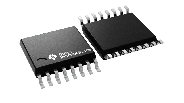
Images are for reference only , Please refer to the product datasheet
SN74LVC574APWG4
Octal Edge-Triggered D-Type Flip-Flop With 3-State Outputs
Manufacturer:
Manufacturer NO:
SN74LVC574APWG4
copy
Product SN:
10481-SN74LVC574APWG4
copy
Package/Case:
-
copy
Manufacturer Lead Time:
-
copy
Datasheet:
Detailed Descripition:
Balanced outputs, Over-voltage tolerant inputs, Partial power down (Ioff), Very high speed (tpd 5-10ns)
copy
Product Application Field:None
Product Application Field:None
Documents & Media
Datasheets PDF SN74LVC574APWG4 Datasheet PDF
Product Description
- Operate From 1.65 V to 3.6 V
- Inputs Accept Voltages to 5.5 V
- Specified From -40°C to 85°C, -40°C to 125°C, and -55°C to 125°C
- Max tpd of 7 ns at 3.3 V
- Typical VOLP (Output Ground Bounce)
<0.8 V at VCC = 3.3 V, TA = 25°C - Typical VOHV (Output VOH Undershoot)
>2 V at VCC = 3.3 V, TA = 25°C - Support Mixed-Mode Signal Operation on All Ports (5-V Input/Output Voltage With 3.3-V VCC)
- Ioff Supports Partial-Power-Down Mode Operation
- Latch-Up Performance Exceeds 250 mA Per JESD 17
- ESD Protection Exceeds JESD 22
- 2000-V Human-Body Model (A114-A)
- 200-V Machine Model (A115-A)
- 1000-V Charged-Device Model (C101)
0 In Stock
Finding Goods Through Sales
Want the lower wholesale price? Please send RFQ, we will respond immediately
Product price
No prices available at the moment
For more SN74LVC574APWG4 prices, contact customer service to get a discount!
You May Also Like

0 In Stock
Finding Goods Through Sales
Want the lower wholesale price? Please send RFQ, we will respond immediately
Product price
No prices available at the moment
For more SN74LVC574APWG4 prices, contact customer service to get a discount!
Home
Chat
Compare
Add To RFQ