
Sign in
Sign up


Images are for reference only , Please refer to the product datasheet
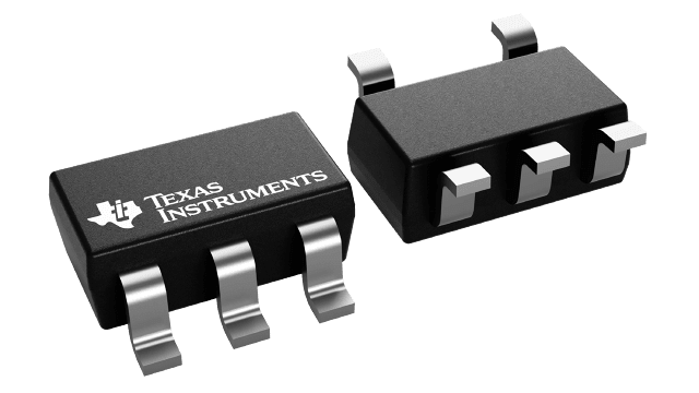
TL331IDBVRQ1
Automotive Catalog Single Differential Comparator
Manufacturer:
Manufacturer NO:
TL331IDBVRQ1
copy
Product SN:
10474-TL331IDBVRQ1
copy
Package/Case:
SOT-23 (DBV)-5
copy
Manufacturer Lead Time:
-
copy
Datasheet:
Detailed Descripition:
-
copy
Product Application Field:None
Product Application Field:None
Documents & Media
Datasheets PDF TL331IDBVRQ1 Datasheet PDF
Product Description
- Qualified for automotive applications
- AEC-Q100 qualified with the following results:
- Device temperature grade 1: –40°C to 125°C ambient operating temperature range (B and Q versions)
- Device temperature grade 3: –40°C to 85°C ambient operating temperature range (I version)
- Device HBM ESD classification level 2
- Device CDM ESD classification level C5
- NEW TL331B-Q1 and TL391B-Q1
- Wide range of supply voltage, 2 V to 36 V
- Low supply-current drain independent of supply voltage: 0.43 mA Typ (B version)
- Low input bias current, 3.5 nA typ (B version)
- Low input offset voltage, 0.37 mV typ (B Version)
- Differential input voltage range equal to maximum-rated supply voltage, ±36 V
- Input range includes ground
- TL391B-Q1 provides an alternate pinout
- Output compatible With TTL, MOS and CMOS
0 In Stock
Finding Goods Through Sales
Want the lower wholesale price? Please send RFQ, we will respond immediately
Product price
Qty
Unit Price
Ext Price
1000
$0.132
$132
For more TL331IDBVRQ1 prices, contact customer service to get a discount!
You May Also Like

0 In Stock
Finding Goods Through Sales
Want the lower wholesale price? Please send RFQ, we will respond immediately
Product price
Qty
Unit Price
Ext Price
1000
$0.132
$132
For more TL331IDBVRQ1 prices, contact customer service to get a discount!
Home
Chat
Compare
Add To RFQ