
Sign in
Sign up


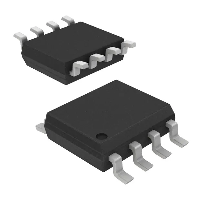
Images are for reference only , Please refer to the product datasheet
TLC3555QDRQ1
Automotive high-speed CMOS timer with integrated reset pull up
Manufacturer:
Manufacturer NO:
TLC3555QDRQ1
copy
Product SN:
10431-TLC3555QDRQ1
copy
Package/Case:
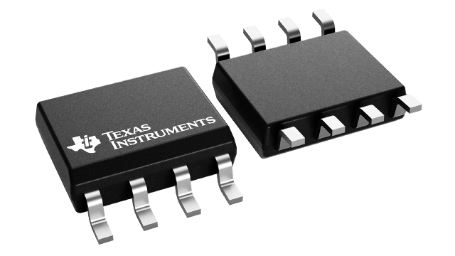
SOIC (D)-8
copy
Manufacturer Lead Time:
-
copy
Datasheet:
Detailed Descripition:
-
copy
Product Application Field:None
Product Application Field:None
Documents & Media
Datasheets PDF TLC3555QDRQ1 Datasheet PDF
Product Description
- AEC-Q100 qualified for automotive applications:
- Temperature grade 1: –40°C to +125°C, TA
- Functional Safety-Capable
- Documentation available to aid functional safety system design
- Very-low power consumption
- 1mW (typical) at VDD = 5V
- Astable operation up to 3MHz
- CMOS output capable of swinging rail to rail
- High-output-current capability
- Sink 200mA
- Source 50mA
- Output fully compatible with CMOS, TTL, and MOS logic
- Integrated RESET pullup to VDD
- Power-on reset to known state
- Integrated thermal shutdown protection
- Single-supply operation from 1.5V to 18V
0 In Stock
Finding Goods Through Sales
Want the lower wholesale price? Please send RFQ, we will respond immediately
Product price
Qty
Unit Price
Ext Price
1000
$0.3
$300
For more TLC3555QDRQ1 prices, contact customer service to get a discount!
You May Also Like


0 In Stock
Finding Goods Through Sales
Want the lower wholesale price? Please send RFQ, we will respond immediately
Product price
Qty
Unit Price
Ext Price
1000
$0.3
$300
For more TLC3555QDRQ1 prices, contact customer service to get a discount!
Home
Chat
Compare
Add To RFQ