compareIcon
loading
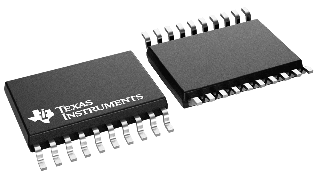
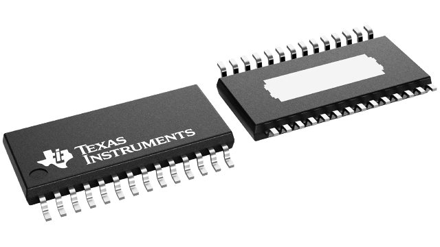
Images are for reference only , Please refer to the product datasheet

TLC6C5912QPWRQ1

Automotive power logic 12-bit Shift Register LED driver

Manufacturer NO:

TLC6C5912QPWRQ1

copy
Product SN:

10509-TLC6C5912QPWRQ1

copy
Package/Case:

TSSOP (PW)-20

copy
Manufacturer Lead Time:
-
copy
Detailed Descripition:

Thermal shutdown

copy

Product Application Field:None

Documents & Media

The PDF does not currently support to preview.Please click on this file to view it

Product Description

The TLC6C5912-Q1 is a monolithic, medium-voltage, low-current power 12-bit shift register designed for use in systems that require relatively moderate load power, such as LEDs.

This device contains a 12-bit serial-in, parallel-out shift register that feeds a 12-bit D-type storage register. Data transfers through both the shift and storage registers on the rising edge of the shift-register clock (SRCK) and the register clock (RCK), respectively. The storage register transfers data to the output buffer when shift register clear (CLR) is high. A low on CLR clears all registers in the device. Holding the output enable (G) high holds all data in the output buffers low, and all drain outputs are off. Holding G low makes data from the storage register transparent to the output buffers.

When data in the output buffers is low, the DMOS transistor outputs are off. When data is high, the DMOS transistor outputs have sink-current capability. The serial output (SER OUT) clocks out of the device on the falling edge of SRCK to provide additional hold time for cascaded applications. This provides improved performance for applications where clock signals may be skewed, devices are not located near one another, or the system must tolerate electromagnetic interference. The device contains a built-in thermal shutdown protection.

Outputs are low-side, open-drain DMOS transistors with output ratings of 40 V and 50-mA continuous sink-current capabilities when VCC = 5 V. The current limit decreases as the junction temperature increases for additional device protection. The device also provides up to 2000 V of ESD protection when tested using the human-body model and 200 V when tested using the machine model.

The TLC6C5912-Q1 characterization is for operation over the operating ambient temperature range of −40°C to 125°C.


  • Qualified for Automotive Applications
  • Wide VCC Range from 3 V to 5.5 V
  • Output Maximum Rating of 40 V
  • Twelve Power DMOS Transistor Outputs of
    50-mA Continuous Current With VCC = 5 V
  • Thermal Shutdown Protection
  • Enhanced Cascading for Multiple Stages
  • All Registers Cleared With Single Input
  • Low Power Consumption
  • Slow Switching Time (tr and tf), Which Helps Significantly With Reducing EMI
  • 20-Pin TSSOP-PW Package
  • 20-Pin DW Package
0 In Stock
Finding Goods Through Sales
Want the lower wholesale price? Please send RFQ, we will respond immediately

Product price

Qty
Unit Price
Ext Price
1000
$0.5
$500
For more TLC6C5912QPWRQ1 prices, contact customer service to get a discount!