
Sign in
Sign up


Images are for reference only , Please refer to the product datasheet
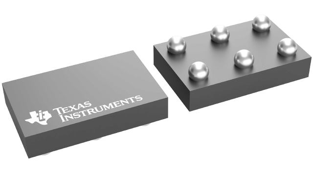
TPS22925CNYPHT
6-DSBGA 3.6-V, 3-A, 9.2-mΩ load switch with output discharge
Manufacturer:
Manufacturer NO:
TPS22925CNYPHT
copy
Product SN:
10514-TPS22925CNYPHT
copy
Package/Case:
DSBGA (YPH)-6
copy
Manufacturer Lead Time:
6 Weeks
copy
Datasheet:
Detailed Descripition:
Quick output discharge, Reverse current protection
copy
Product Application Field:None
Product Application Field:None
Environmental & Export Classifications
RoHS Status
ROHS3 Compliant
Moisture Sensitivity Level (MSL)
1 (Unlimited)
REACH Status
REACH Unaffected
ECCN
EAR99
HTSUS
8542.39.0001
Documents & Media
Datasheets PDF TPS22925CNYPHT Datasheet PDF
Product Description
- Input Voltage Range: 0.65 V to 3.6 V
- On-Resistance
- RON = 9.2 mΩ at VIN = 3.6 V
- RON = 9.2 mΩ at VIN = 1.8 V
- RON = 10.2 mΩ at VIN = 1 V
- RON = 13.1 mΩ at VIN = 0.65 V
- 3-A Maximum Continuous Switch Current
- Quiescent Current, IQ,VIN = 29 µA at VIN = 3.6 V
- Low Control Input Threshold Enables 1.5-, 1.8-, 2.5-, or 3.3-V Logic
- Controlled Slew Rate
- tR = 97 µs at VIN = 3.6 V (TPS22925Bx)
- tR = 810 µs at VIN = 3.6 V (TPS22925Cx)
- Reverse Current Blocking (When Disabled)
- Quick Output Discharge (QOD) (TPS22925B and TPS22925C only)
- Wafer Chip Scale Package:
- 0.9 mm × 1.4 mm, 0.5-mm Pitch, 0.4-mm Height
- ESD Performance Tested per JESD 22
- 2-kV HBM and 1-kV CDM
6000 In Stock
Can Ship lmmediately
Want the lower wholesale price? Please send RFQ, we will respond immediately
Product price
Qty
Unit Price
Ext Price
1000
$0.373
$373
For more TPS22925CNYPHT prices, contact customer service to get a discount!
You May Also Like


6000 In Stock
Can Ship lmmediately
Want the lower wholesale price? Please send RFQ, we will respond immediately
Product price
Qty
Unit Price
Ext Price
1000
$0.373
$373
For more TPS22925CNYPHT prices, contact customer service to get a discount!
Home
Chat
Compare
Add To RFQ