
Sign in
Sign up


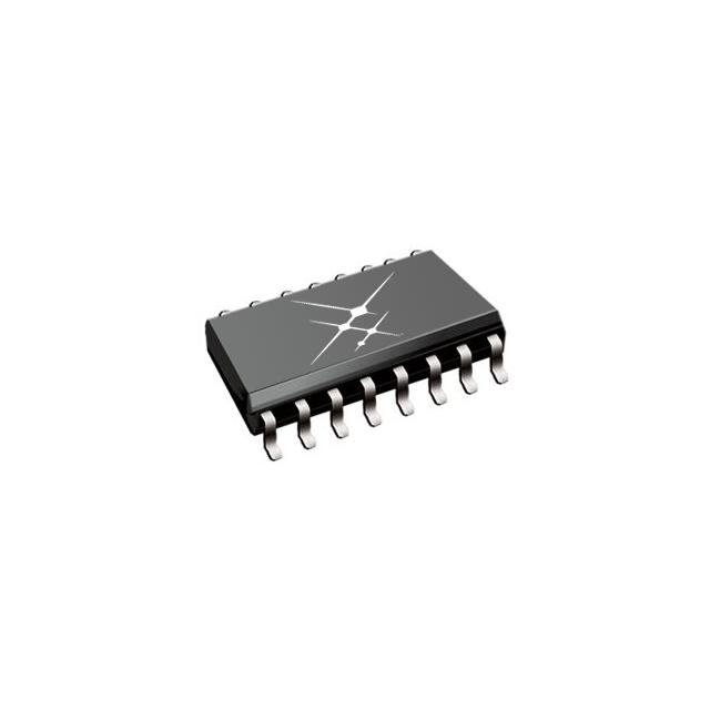
Images are for reference only , Please refer to the product datasheet
UCC20225AQNPLTQ1
13-VLGA (5x5) Automotive 2.5kVrms, 4A/6A dual-channel isolated gate driver w/ single PWM input, 5V UVLO in LGA pkg
Manufacturer:
Manufacturer NO:
UCC20225AQNPLTQ1
copy
Product SN:
10531-UCC20225AQNPLTQ1
copy
Package/Case:
VLGA (NPL)-13
copy
Manufacturer Lead Time:
12 Weeks
copy
Datasheet:
Detailed Descripition:
Disable, Programmable dead time
copy
Product Application Field:None
Product Application Field:None
Environmental & Export Classifications
RoHS Status
ROHS3 Compliant
Moisture Sensitivity Level (MSL)
3 (168 Hours)
REACH Status
REACH Unaffected
ECCN
EAR99
HTSUS
8542.39.0001
Documents & Media
Datasheets PDF UCC20225AQNPLTQ1 Datasheet PDF
Product Description
- AEC Q100 qualified with:
- Device temperature grade 1
- Device HBM ESD classification level H2
- Device CDM ESD classification level C6
- Single PWM input, dual output
- Resistor-programmable dead time
- 4-A peak source, 6-A peak sink output
- CMTI greater than 100-V/ns
- Switching parameters:
- 19-ns typical propagation delay
- 5-ns maximum delay matching
- 6-ns maximum pulse-width distortion
- 3-V to 18-V input VCCI range
- Up to 25-V VDD with 5V and 8-V UVLO Options
- Rejects input transients shorter than 5-ns
- TTL and CMOS compatible inputs
- 5-mm x 5-mm space-saving LGA-13 Package
- Safety-related certifications:
- 3535-VPK isolation per VDE V 0884-11:2017
- 2500-VRMS isolation for 1 minute per UL 1577
- CQC Certification per GB4943.1-2011
0 In Stock
Finding Goods Through Sales
Want the lower wholesale price? Please send RFQ, we will respond immediately
Product price
Qty
Unit Price
Ext Price
1000
$2.657
$2657
For more UCC20225AQNPLTQ1 prices, contact customer service to get a discount!
You May Also Like


0 In Stock
Finding Goods Through Sales
Want the lower wholesale price? Please send RFQ, we will respond immediately
Product price
Qty
Unit Price
Ext Price
1000
$2.657
$2657
For more UCC20225AQNPLTQ1 prices, contact customer service to get a discount!
Home
Chat
Compare
Add To RFQ