
Sign in
Sign up


Images are for reference only , Please refer to the product datasheet
V62/06649-01XE
Enhanced Product 16-Bit Transparent D-Type Latch With 3-State Outputs
Manufacturer:
Manufacturer NO:
V62/06649-01XE
copy
Product SN:
10484-V62/06649-01XE
copy
Package/Case:
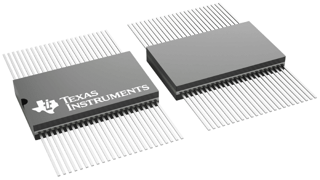
SSOP (DL)-48
copy
Manufacturer Lead Time:
-
copy
Datasheet:
Detailed Descripition:
Balanced outputs, Flow-through pinout, Over-voltage tolerant inputs, Partial power down (Ioff), Very high speed (tpd 5-10ns)
copy
Product Application Field:None
Product Application Field:None
Documents & Media
Datasheets PDF V62/06649-01XE Datasheet PDF
Product Description
- Member of the Texas Instruments Widebus™ Family
- Operates From 1.65 V to 3.6 V
- Inputs Accept Voltages to 5.5 V
- Max tpd of 4.2 ns at 3.3 V
- Typical VOLP (Output Ground Bounce) <0.8 V at VCC = 3.3 V, TA = 25°C
- Typical VOHV (Output VOH Undershoot) >2 V at VCC = 3.3 V, TA = 25°C
- Ioff Supports Partial-Power-Down Mode Operation
- Supports Mixed-Mode Signal Operation (5-V Input and Output Voltages With 3.3-V VCC)
- Latch-Up Performance Exceeds 100 mA Per JESD 78, Class II
- ESD Protection Exceeds JESD 22
- 2000-V Human-Body Model (A114-A)
- 1000-V Charged-Device Model (C101)
0 In Stock
Finding Goods Through Sales
Want the lower wholesale price? Please send RFQ, we will respond immediately
Product price
Qty
Unit Price
Ext Price
1000
$1.597
$1597
For more V62/06649-01XE prices, contact customer service to get a discount!
You May Also Like


0 In Stock
Finding Goods Through Sales
Want the lower wholesale price? Please send RFQ, we will respond immediately
Product price
Qty
Unit Price
Ext Price
1000
$1.597
$1597
For more V62/06649-01XE prices, contact customer service to get a discount!
Home
Chat
Compare
Add To RFQ