
Sign in
Sign up


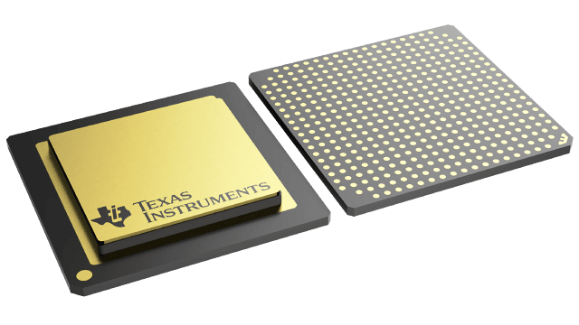
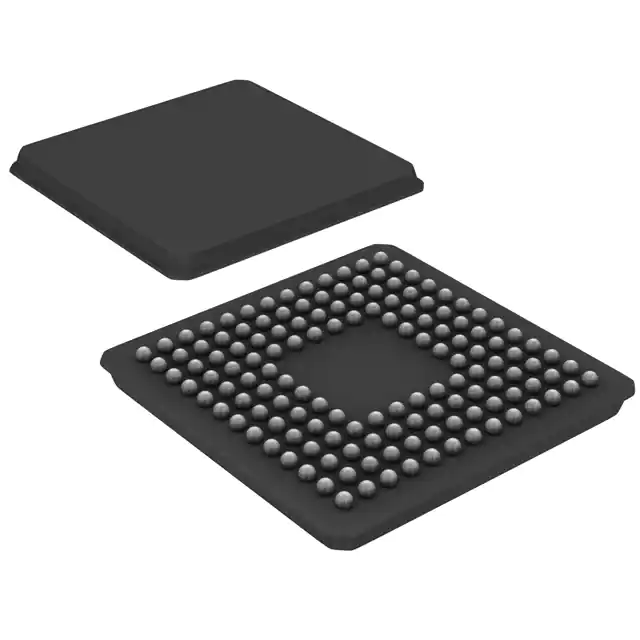
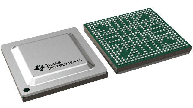
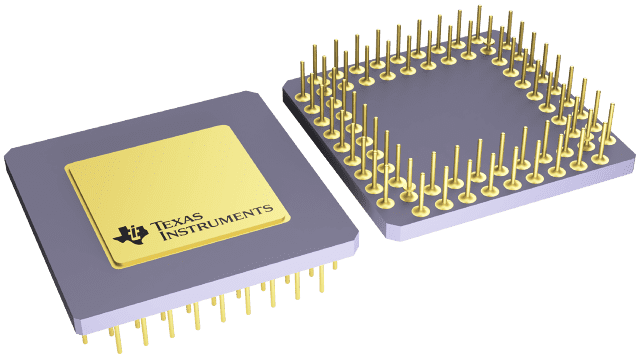
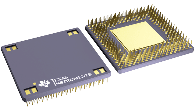
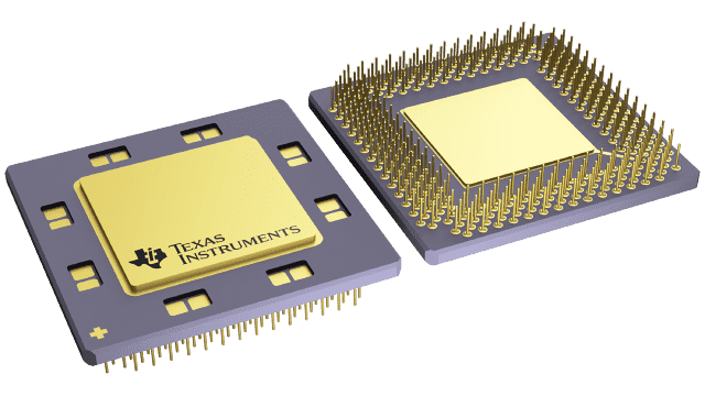
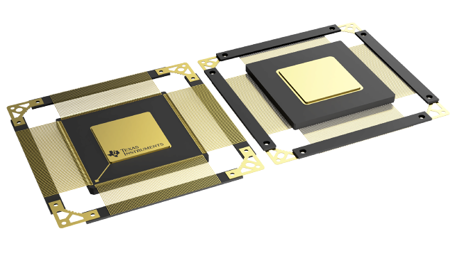
Images are for reference only , Please refer to the product datasheet
5962-0051001QXA
Military grade C62x fixed point DSP - ceramic package
Manufacturer:
Manufacturer NO:
5962-0051001QXA
copy
Product SN:
10442-5962-0051001QXA
copy
Package/Case:
CFCBGA (GLP)-429
copy
Manufacturer Lead Time:
-
copy
Datasheet:
Detailed Descripition:
-
copy
Product Application Field:None
Product Application Field:None
Documents & Media
Datasheets PDF 5962-0051001QXA Datasheet PDF
Product Description
- High-Performance Fixed-Point Digital Signal
Processor (DSP) SMJ320C62x™- 5-ns Instruction Cycle Time
- 200-MHz Clock Rate
- Eight 32-Bit Instructions/Cycle
- 1600 Million Instructions per Second (MIPS)
- 429-Pin Ball Grid Array (BGA) Package (GLP
Suffix) - VelociTI™ Advanced Very-Long-Instruction-Word
(VLIW) C62x DSP Core- Eight Highly-Independent Functional Units:
- Six Arithmetic Logic Units (ALUs) (32-/40-
Bit) - Two 16-Bit Multipliers (32-Bit Result)
- Six Arithmetic Logic Units (ALUs) (32-/40-
- Load-Store Architecture With 32 32-Bit
General-Purpose Registers - Instruction Packing Reduces Code Size
- All Instructions Conditional
- Eight Highly-Independent Functional Units:
- Instruction Set Features
- Byte-Addressable (8-, 16-, 32-Bit Data)
- 8-Bit Overflow Protection
- Saturation
- Bit-Field Extract, Set, Clear
- Bit-Counting
- Normalization
- 7Mb On-Chip SRAM
- 3Mb Internal Program/Cache (96K 32-Bit
Instructions) - 4Mb Dual-Access Internal Data (512KB)
- Organized as Two 256KB Blocks for Improved
Concurrency
- 3Mb Internal Program/Cache (96K 32-Bit
- Flexible Phase-Locked-Loop (PLL) Clock
Generator - 32-Bit External Memory Interface (EMIF)
- Glueless Interface to Synchronous Memories:
SDRAM or SBSRAM - Glueless Interface to Asynchronous Memories:
SRAM and EPROM - 52MB Addressable External Memory Space
- Glueless Interface to Synchronous Memories:
- Four-Channel Bootloading Direct-Memory-Access
(DMA) Controller With an Auxiliary Channel - 32-Bit Expansion Bus − Glueless/Low-Glue
- Glueless/Low-Glue Interface to Popular
Synchronous or Asynchronous Microprocessor
Buses - Master/Slave Functionality
- Glueless Interface to Synchronous FIFOs and
Asynchronous Peripherals - Three Multichannel Buffered Serial Ports
(McBSPs)- Direct Interface to T1/E1, MVIP, SCSA
Framers - ST-Bus-Switching Compatible
- Up to 256 Channels Each
- AC97-Compatible
- Serial-Peripheral Interface (SPI) Compatible
(Motorola®)
- Direct Interface to T1/E1, MVIP, SCSA
- Two 32-Bit General-Purpose Timers
- IEEE-1149.1 (JTAG(2)) Boundary-Scan-
Compatible - 0.15-µm/5-Level Metal Process
- CMOS Technology
- 3.3-V I/Os, 1.5-V Internal
0 In Stock
Finding Goods Through Sales
Want the lower wholesale price? Please send RFQ, we will respond immediately
Product price
Qty
Unit Price
Ext Price
1000
$1041.977
$1041977
For more 5962-0051001QXA prices, contact customer service to get a discount!
You May Also Like


0 In Stock
Finding Goods Through Sales
Want the lower wholesale price? Please send RFQ, we will respond immediately
Product price
Qty
Unit Price
Ext Price
1000
$1041.977
$1041977
For more 5962-0051001QXA prices, contact customer service to get a discount!
Home
Chat
Compare
Add To RFQ