
Sign in
Sign up


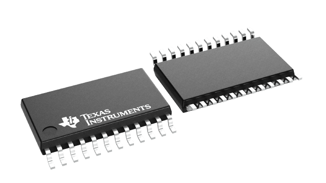
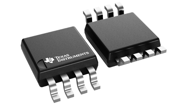
Images are for reference only , Please refer to the product datasheet
ADC122S625CIMMX/NOPB
Dual 12-Bit, 50 kSPS to 200 kSPS, Simultaneous Sampling A/D Converter
Manufacturer:
Manufacturer NO:
ADC122S625CIMMX/NOPB
copy
Product SN:
10435-ADC122S625CIMMX/NOPB
copy
Package/Case:
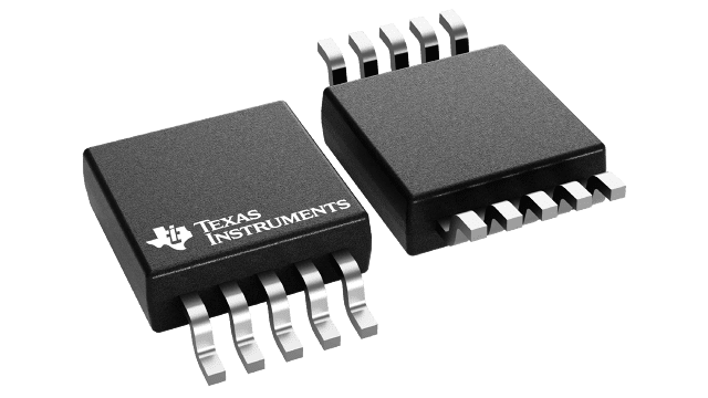
VSSOP (DGS)-10
copy
Manufacturer Lead Time:
-
copy
Datasheet:
Detailed Descripition:
-
copy
Product Application Field:None
Product Application Field:None
Documents & Media
Datasheets PDF ADC122S625CIMMX/NOPB Datasheet PDF
Product Description
- True Simultaneous Sampling Differential Inputs
- Specified Performance from 50 kSPS to 200 kSPS
- External Reference
- Wide Input Common-Mode Voltage Range
- Single High-Speed Serial Data Output
- Operating Temperature Range of −40°C to +105°C
- SPI/QSPI/MICROWIRE/DSP Compatible Serial Interface
- Conversion Rate: 50 kSPS to 200 kSPS
- INL: ±1 LSB (max)
- DNL: ±0.95 LSB (max)
- SNR: 71 dBc (min)
- THD: -72 dBc (min)
- ENOB: 11.25 bits (min)
- Power Consumption at 200 kSPS
- Converting, VA = 5V, VREF = 2.5V: 8.6 mW (typ)
- Power-Down, VA = 5V, VREF = 2.5V: 2.6 µW (typ)
0 In Stock
Finding Goods Through Sales
Want the lower wholesale price? Please send RFQ, we will respond immediately
Product price
Qty
Unit Price
Ext Price
1000
$3.025
$3025
For more ADC122S625CIMMX/NOPB prices, contact customer service to get a discount!
You May Also Like

0 In Stock
Finding Goods Through Sales
Want the lower wholesale price? Please send RFQ, we will respond immediately
Product price
Qty
Unit Price
Ext Price
1000
$3.025
$3025
For more ADC122S625CIMMX/NOPB prices, contact customer service to get a discount!
Home
Chat
Compare
Add To RFQ