
Sign in
Sign up


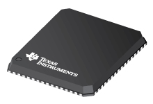
Images are for reference only , Please refer to the product datasheet
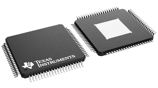
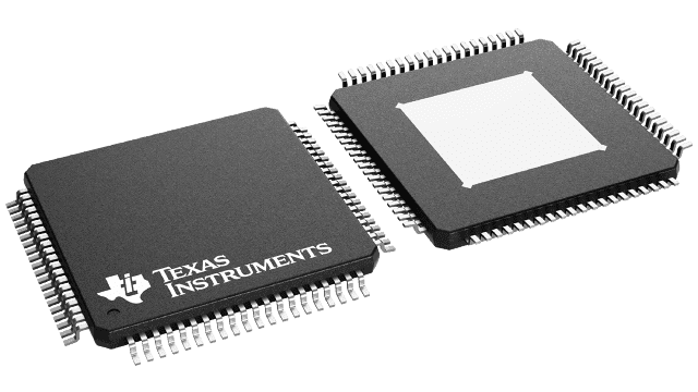
ADS5270IPFP
Eight-Channel, 12-Bit, 40-MSPS Analog-to-Digital Converter (ADC)
Manufacturer:
Manufacturer NO:
ADS5270IPFP
copy
Product SN:
10435-ADS5270IPFP
copy
Package/Case:
HTQFP (PFP)-80
copy
Manufacturer Lead Time:
-
copy
Datasheet:
Detailed Descripition:
Low Power
copy
Product Application Field:None
Product Application Field:None
Documents & Media
Datasheets PDF ADS5270IPFP Datasheet PDF
Product Description
- Maximum Sample Rate: 40MSPS
- 12-Bit Resolution
- No Missing Codes
- Total Power Dissipation:
Internal Reference: 888mW
External Reference: 822mW - CMOS Technology
- Simultaneous Sample-and-Hold
- 70.5dB SNR at 10MHz IF
- 3.3V Digital/Analog Supply
- Serialized LVDS Outputs
- Integrated Frame and Bit Patterns
- Option to Double LVDS Clock Output Currents
- Four Current Modes for LVDS
- Pin- and Format-Compatible Family
- TQFP-80 PowerPAD Package
0 In Stock
Finding Goods Through Sales
Want the lower wholesale price? Please send RFQ, we will respond immediately
Product price
Qty
Unit Price
Ext Price
1000
$66.417
$66417
For more ADS5270IPFP prices, contact customer service to get a discount!
You May Also Like

0 In Stock
Finding Goods Through Sales
Want the lower wholesale price? Please send RFQ, we will respond immediately
Product price
Qty
Unit Price
Ext Price
1000
$66.417
$66417
For more ADS5270IPFP prices, contact customer service to get a discount!
Home
Chat
Compare
Add To RFQ