
Sign in
Sign up


Images are for reference only , Please refer to the product datasheet
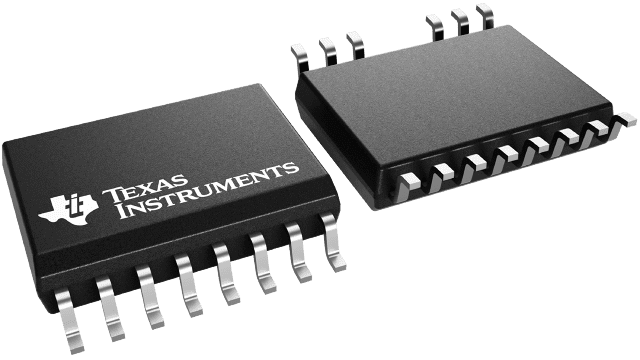
PUCC21530QDWKQ1
Automotive 4-A, 6-A, 5.7-kVRMS, isolated dual-channel gate driver with EN and DT pins for IGBT/SiC
Manufacturer:
Manufacturer NO:
PUCC21530QDWKQ1
copy
Product SN:
10506-PUCC21530QDWKQ1
copy
Package/Case:
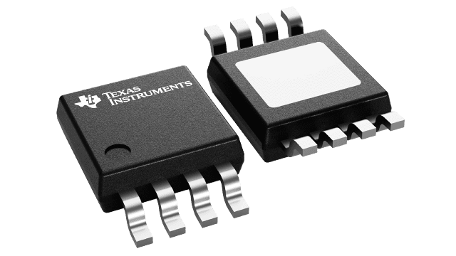
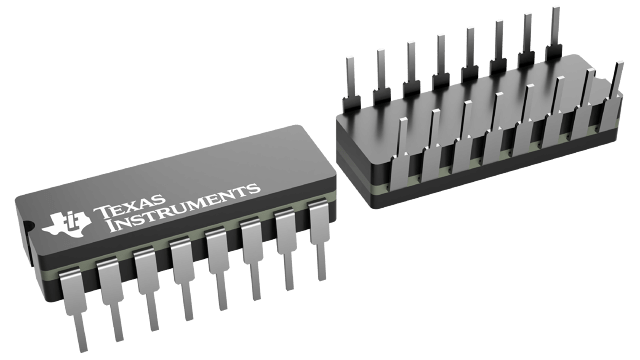
SOIC (DWK)-14
copy
Manufacturer Lead Time:
-
copy
Datasheet:
Detailed Descripition:
Enable, Programmable dead time
copy
Product Application Field:None
Product Application Field:None
Documents & Media
Datasheets PDF PUCC21530QDWKQ1 Datasheet PDF
Product Description
- AEC-Q100 qualified with:
- Device temperature grade 1
- Device HBM ESD classification level H2
- Device CDM ESD classification level C6
- Functional Safety Quality-Managed
- Documentation available to aid functional safety system design
- Universal: dual low-side, dual high-side or half-bridge driver
- Wide body SOIC-14 (DWK) package
- 3.3-mm spacing between driver channels
- Switching parameters:
- 19-ns typical propagation delay
- 10-ns minimum pulse width
- 5-ns maximum delay matching
- 6-ns maximum pulse-width distortion
- Common-mode transient immunity (CMTI) greater than 100-V/ns
- Isolation barrier life >40 years
- 4-A peak source, 6-A peak sink output
- TTL and CMOS compatible inputs
- 3-V to 18-V input VCCI range
- Up to 25-V VDD output drive supply
- 8-V and 12-V VDD UVLO options
- Programmable overlap and dead time
- Rejects input pulses and noise transients shorter than 5 ns
- Operating temperature range –40 to +125°C
- Safety-related certifications:
- 8000-VPK isolation per DIN V VDE V 0884-11 :2017-01
- 5.7-kVRMS isolation for 1 minute per UL 1577
- CSA certification per IEC 60950-1, IEC 62368-1, IEC 61010-1 and IEC 60601-1 end equipment standards
- CQC certification per GB4943.1-2011
0 In Stock
Finding Goods Through Sales
Want the lower wholesale price? Please send RFQ, we will respond immediately
Product price
Qty
Unit Price
Ext Price
1000
$3.59
$3590
For more PUCC21530QDWKQ1 prices, contact customer service to get a discount!
You May Also Like


0 In Stock
Finding Goods Through Sales
Want the lower wholesale price? Please send RFQ, we will respond immediately
Product price
Qty
Unit Price
Ext Price
1000
$3.59
$3590
For more PUCC21530QDWKQ1 prices, contact customer service to get a discount!
Home
Chat
Compare
Add To RFQ