
Sign in
Sign up


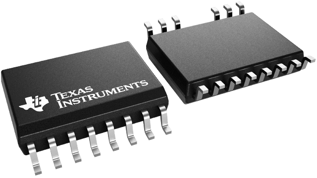
Images are for reference only , Please refer to the product datasheet
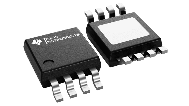
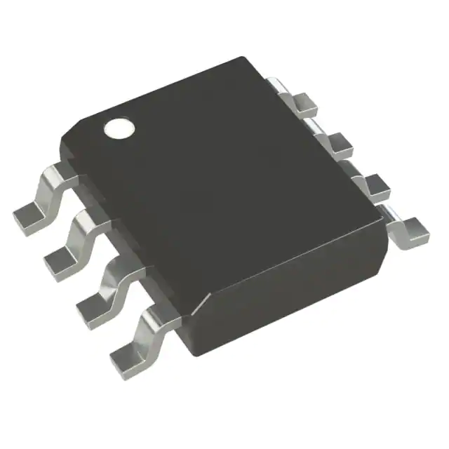
UCC27524DGN
5-A/5-A dual-channel gate driver with 5-V UVLO, enable, and 1-ns delay Matching
Manufacturer:
Manufacturer NO:
UCC27524DGN
copy
Product SN:
10506-UCC27524DGN
copy
Package/Case:
HVSSOP (DGN)-8
copy
Manufacturer Lead Time:
-
copy
Datasheet:
Detailed Descripition:
Enable pin
copy
Product Application Field:None
Product Application Field:None
Documents & Media
Datasheets PDF UCC27524DGN Datasheet PDF
Product Description
- Industry-standard pin out
- Two independent gate-drive channels
- 5A peak source and sink-drive current
- Independent-enable function for each output
- TTL and CMOS compatible logic threshold independent of supply voltage
- Hysteretic-logic thresholds for high noise immunity
- Ability to handle negative voltages (–5V) at inputs
- Inputs and enable pin-voltage levels not restricted by VDD pin bias supply voltage
- 4.5V to 18V single-supply range
- Outputs held low during VDD-UVLO (ensures glitch-free operation at power up and power down)
- Fast propagation delays (17ns typical)
- Fast rise and fall times (6ns and 10ns typical)
- 1ns typical delay matching between two channels
- Two outputs are paralleled for higher drive current
- Outputs held in low when inputs floating
- SOIC-8, HVSSOP-8 PowerPAD™ package options
- Operating junction temperature range of –40 to 150°C
0 In Stock
Finding Goods Through Sales
Want the lower wholesale price? Please send RFQ, we will respond immediately
Product price
Qty
Unit Price
Ext Price
1000
$0.855
$855
For more UCC27524DGN prices, contact customer service to get a discount!
You May Also Like


0 In Stock
Finding Goods Through Sales
Want the lower wholesale price? Please send RFQ, we will respond immediately
Product price
Qty
Unit Price
Ext Price
1000
$0.855
$855
For more UCC27524DGN prices, contact customer service to get a discount!
Home
Chat
Compare
Add To RFQ