
Sign in
Sign up


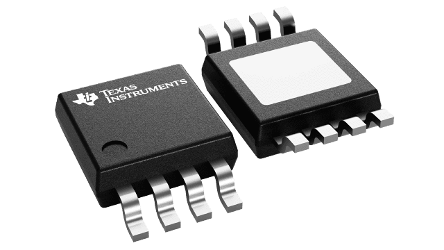
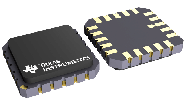
Images are for reference only , Please refer to the product datasheet
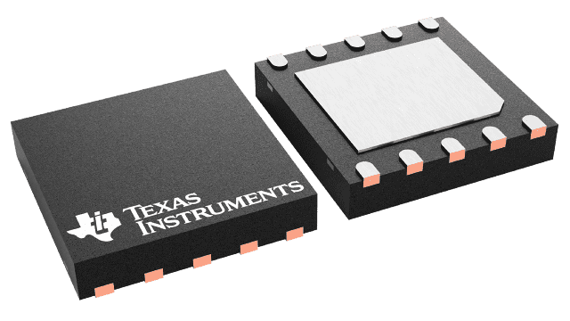
UCC27212DPRR
10-WSON (4x4) 4-A, 120-V half bridge gate driver with 5-V UVLO and negative voltage handling
Manufacturer:
Manufacturer NO:
UCC27212DPRR
copy
Product SN:
10506-UCC27212DPRR
copy
Package/Case:
WSON (DPR)-10
copy
Manufacturer Lead Time:
8 Weeks
copy
Datasheet:
Detailed Descripition:
Half-Bridge Gate Driver IC Non-Inverting 10-WSON (4x4)
copy
Product Application Field:None
Product Application Field:None
Environmental & Export Classifications
RoHS Status
ROHS3 Compliant
Moisture Sensitivity Level (MSL)
2 (1 Year)
REACH Status
REACH Unaffected
ECCN
EAR99
HTSUS
8542.39.0001
Documents & Media
Datasheets PDF UCC27212DPRR Datasheet PDF
Product Description
- 4-A Sink, 4-A Source Output Currents
- Maximum Boot Voltage 120-V DC
- 7-V to 17-V VDD Operating Range
- 20-V ABS Maximum VDD Operating Range
- 5-V Turn-off Under Voltage Lockout (UVLO)
- Input Pins Can Tolerate –10 V to +20 V
- 7.2-ns Rise and 5.5-ns Fall Time (1000-pF Load)
- 20-ns Typical Propagation Delay
- 4-ns Typical Delay Matching
- Specified from –40°C to +140°C
0 In Stock
Finding Goods Through Sales
Want the lower wholesale price? Please send RFQ, we will respond immediately
Product price
Qty
Unit Price
Ext Price
1000
$4.114
$4114
For more UCC27212DPRR prices, contact customer service to get a discount!
You May Also Like


0 In Stock
Finding Goods Through Sales
Want the lower wholesale price? Please send RFQ, we will respond immediately
Product price
Qty
Unit Price
Ext Price
1000
$4.114
$4114
For more UCC27212DPRR prices, contact customer service to get a discount!
Home
Chat
Compare
Add To RFQ