
Sign in
Sign up


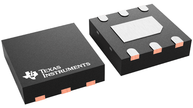
Images are for reference only , Please refer to the product datasheet
V62/13608-01XE
Enhanced Product 4-A/8-A single-channel gate driver with 5-V UVLO in SON package
Manufacturer:
Manufacturer NO:
V62/13608-01XE
copy
Product SN:
10506-V62/13608-01XE
copy
Package/Case:
WSON (DRS)-6
copy
Manufacturer Lead Time:
-
copy
Datasheet:
Detailed Descripition:
Hysteretic Logic
copy
Product Application Field:None
Product Application Field:None
Documents & Media
Datasheets PDF V62/13608-01XE Datasheet PDF
Product Description
- Low-Cost, Gate-Driver Device Offering Superior Replacement
of NPN and PNP Discrete Solutions - 4-A Peak Source and 8-A Peak Sink Asymmetrical Drive
- Strong Sink Current Offers Enhanced Immunity Against Miller Turn On
- Fast Propagation Delays (13-ns typical)
- Fast Rise and Fall Times (9-ns and 7-ns typical)
- 4.5-V to 18-V Single Supply Range
- Outputs Held Low During VDD UVLO (ensures glitch free operation at
power-up and power-down) - TTL and CMOS Compatible Input Logic Threshold,
(independent of supply voltage) - Hysteretic Logic Thresholds for High Noise Immunity
- Dual Input Design (choice of an inverting (IN- pin) or non-inverting
(IN+ pin) driver configuration)- Unused Input Pin can be Used for Enable or Disable Function
- Output Held Low when Input Pins are Floating
- Input Pin Absolute Maximum Voltage Levels Not Restricted by VDD Pin
Bias Supply Voltage - 6-Pin DRS (3mm × 3 mm WSON with exposed thermal pad) Package
- Controlled Baseline
- One Assembly and Test Site
- One Fabrication Site
- Available in Military (–55°C to 125°C) Temperature Range
- Extended Product Life Cycle
- Extended Product-Change Notification
- Product Traceability
0 In Stock
Finding Goods Through Sales
Want the lower wholesale price? Please send RFQ, we will respond immediately
Product price
Qty
Unit Price
Ext Price
1000
$1.625
$1625
For more V62/13608-01XE prices, contact customer service to get a discount!
You May Also Like


0 In Stock
Finding Goods Through Sales
Want the lower wholesale price? Please send RFQ, we will respond immediately
Product price
Qty
Unit Price
Ext Price
1000
$1.625
$1625
For more V62/13608-01XE prices, contact customer service to get a discount!
Home
Chat
Compare
Add To RFQ